Multi-layer RF chip type balance-to-unbalance converter

A chip-type, converter technology, applied in waveguide-type devices, radio transmission systems, coils, etc., can solve problems such as inability to shrink components, and achieve the effect of maintaining stability

Inactive Publication Date: 2003-02-12
IND TECH RES INST
View PDF1 Cites 0 Cited by
  • Summary
  • Abstract
  • Description
  • Claims
  • Application Information

AI Technical Summary

Problems solved by technology

However, in materials with low dielectric constant, it i

Method used


Image

  • Multi-layer RF chip type balance-to-unbalance converter
  • Multi-layer RF chip type balance-to-unbalance converter
  • Multi-layer RF chip type balance-to-unbalance converter

Examples


Embodiment Construction

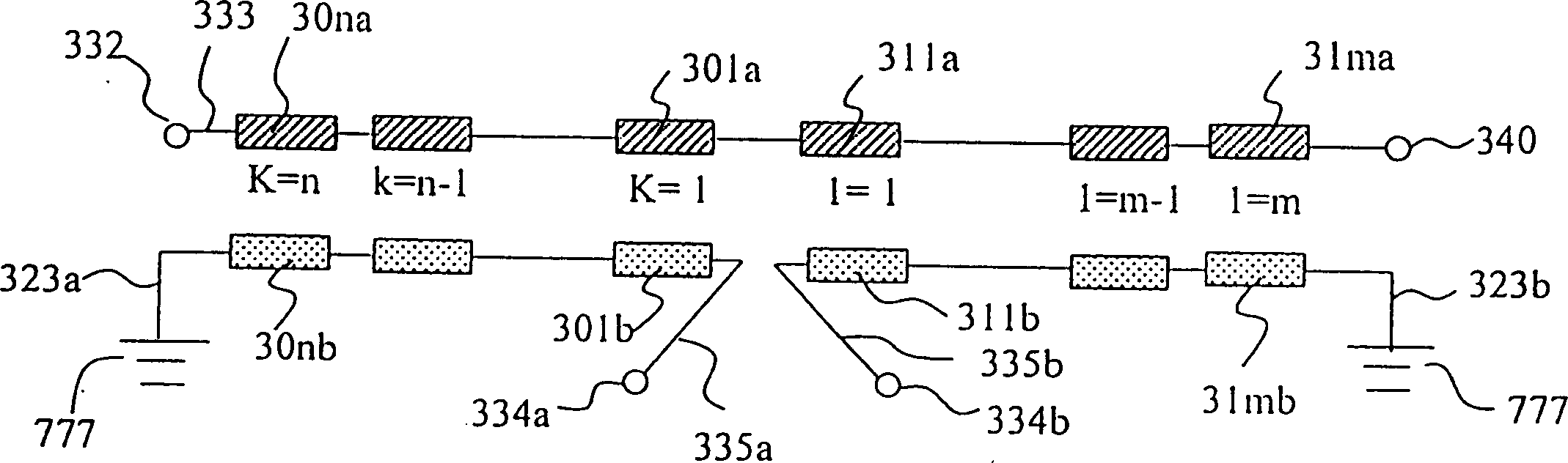
[0049] image 3 It is a schematic diagram of the equivalent circuit of the multi-layer radio frequency chip type balanced to unbalanced converter of the present invention. Such as image 3 As shown, the equivalent circuit 300 of this multilayer radio frequency chip type converter basically consists of an unbalanced port 332, a first balanced port 334a and a second balanced port 334b, and multi-section vertically coupled transmission lines. Each vertically coupled transmission line has a corresponding coupling coefficient, wherein the equivalent circuit has at least two different coupling coefficients. image 3 , a dotted box represents a coupling transmission line, each coupling transmission line is composed of a first line portion and a second line portion, the first line portion and the second line portion are respectively There are two ends. The unbalanced port 332 is an input port, and the two balanced ports 334a and 334b ​​are output ports.

[0050] Depend on image ...


PUM


Abstract

A multi-layer RE chip type balance-unbalance converter has a multi-layer dielectric structure, whose equivalent circuit is composed of an input port, two output ports, and multiple even-section coupled transmission line consisting of a first and a second lines symmetrical to the center point of the said dielectric structure. Its advantage is very good phase and amplitude balance degree.

Description

technical field [0001] The present invention relates to a balance-to-unbalance (balun). In particular, it relates to a multilayer radiofrequency chip-type balun (multilayer radiofrequencv chip balun). The converter is suitable to be made into chip-sized components, and applied in wireless local network (wireless local network) and personal mobile communication equipment. Background technique [0002] A balanced-to-unbalanced converter is a device that converts an unbalanced structure or signal to a balanced structure or signal. A balanced signal is characterized by two signals of equal magnitude but with a phase difference of 180 degrees. Many analog circuits often require balanced output and input, which can not only reduce noise, improve the occurrence of high-order harmonics, but also increase the dynamic range of the circuit. [0003] There are many types of baluns, mainly divided into active and passive. Generally, passive baluns can be classified into three types: ...

Claims


Application Information

Patent Timeline
IPC IPC(8): H01F5/00H01P5/10H01P11/00H04B7/00
Inventor 汤敬文沈志文
Owner IND TECH RES INST
Why Eureka
Try Eureka