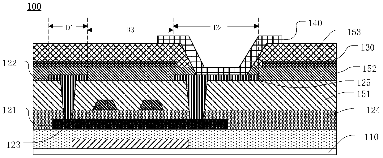
Thin film transistor and manufacturing method thereof, array substrate and display device
A technology of a thin film transistor and a manufacturing method, which are applied in the fields of thin film transistors and their manufacturing methods, array substrates and display devices, can solve the problems of reducing the wiring width of the drain electrode 125, increasing the difficulty of the process, and disconnecting on the slope, and reducing the The effect of climbing the risk of disconnection, increasing the contact area, and increasing the width of the trace
- Summary
- Abstract
- Description
- Claims
- Application Information
AI Technical Summary
Problems solved by technology
Method used
Image
Examples
no. 1 example
[0033] see first figure 2 , figure 2 A cross-sectional view of the thin film transistor 200 according to the first embodiment of the present invention is shown. The thin film transistor 200 includes an active layer 220 , an insulating layer 230 , a first electrode layer 240 and a second electrode layer 250 . In this embodiment, the thin film transistor 200 further includes a gate electrode layer 260 .
[0034] The active layer 220 is a semiconductor layer, which can be formed through processes such as crystallization and doping. The insulating layer 230 is on the active layer 220 . In this embodiment, the insulating layer 230 includes a gate insulating layer 231 and an inter-electrode insulating layer 232 sequentially located on the active layer 220 . In other words, the gate insulating layer 231 is located on the active layer 220 . The inter-electrode insulating layer 232 is located between the gate insulating layer 231 and the second electrode layer 250 . The gate el...
no. 2 example
[0039] see image 3 , image 3 A cross-sectional view of a thin film transistor 300 according to a second embodiment of the present invention is shown. image 3 The thin film transistor 300 shown with figure 2 The thin film transistor 200 shown is similar in structure, and different from the thin film transistor 200, the inter-electrode insulating layer includes a first insulating layer 332A and a second insulating layer 332B on the first insulating layer 332A.
[0040] In the second embodiment, the lower via hole 336 of the first via hole 334 is located in the first insulating layer 332A. The upper via hole 337 of the first via hole 334 is located in the second insulating layer 332B. In other words, the junction of the lower via hole 336 and the upper via hole 337 is the contact interface of the first insulating layer 332A and the second insulating layer 332B. The first electrode layer 340 is located between the first insulating layer 332A and the second insulating layer...
no. 3 example
[0042] see Figure 4 , Figure 4 A cross-sectional view of a thin film transistor 300A according to a third embodiment of the present invention is shown. Figure 4 The thin film transistor 300A shown with image 3 The thin film transistor 300 shown has a similar structure, and the difference with the thin film transistor 300 is that the junction of the upper via hole 337A and the lower via hole 336A of the first via hole 234 is located in the second insulating layer 332B. The bottom surface of the first electrode layer 340 is higher than the contact interface between the first insulating layer 332A and the second insulating layer 332B, and the top surface of the first electrode layer 340 is lower than the top surface of the second insulating layer 332B.
PUM
 Abstract
Description
Claims
Application Information


