Light-emitting device

A light-emitting device and a technology of light-emitting diodes, which are applied in the direction of electrical components, circuits, semiconductor devices, etc., can solve the problems of uneven thickness, yellow halo, and uneven color temperature of the phosphor layer 30 of light-emitting diode chips, so as to reduce the yellow halo phenomenon and Spatial color shift phenomenon, reduce color temperature difference, uniform illumination effect

Inactive Publication Date: 2014-06-18
GENIUS ELECTRONICS OPTICAL CO LTD
View PDF1 Cites 3 Cited by
  • Summary
  • Abstract
  • Description
  • Claims
  • Application Information

AI Technical Summary

Problems solved by technology

[0009] another example figure 2 As shown, it is another traditional light-emitting device. The light-emitting diode chip 20 is arranged on the bottom of a reflective cup 40, and then the fluorescent powder colloid is coated on the top of the light-emitting diode chip 20 by dispensing. Phosphor powder layer 30 is formed in a limited space, however, due to flow, precipitation and surface tension of the phosphor powder colloid, the phosphor powder layer 30 will be convex in the middle, and the periphery will be sunken near the inner side of the reflective cup 40, resulting in the top of the light emitting diode chip 20. The thickness of the phosphor layer 30 is uneven, resulting in the yellow halo phenomenon of uneven color temperature when emitting light

Method used


Image

  • Light-emitting device
  • Light-emitting device
  • Light-emitting device

Examples


Embodiment Construction

[0039] The detailed content and technical description of the present invention are further described by examples, but it should be understood that these examples are only for illustrative purposes, and should not be construed as limitations on the implementation of the present invention.

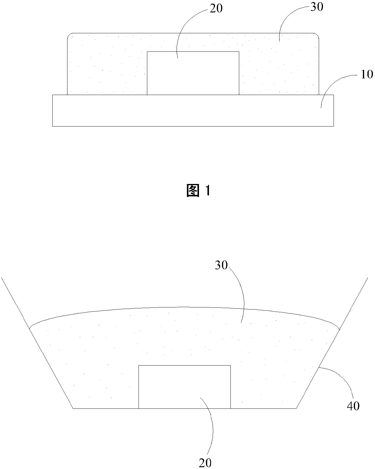
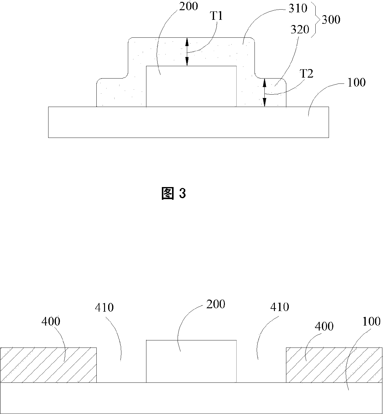
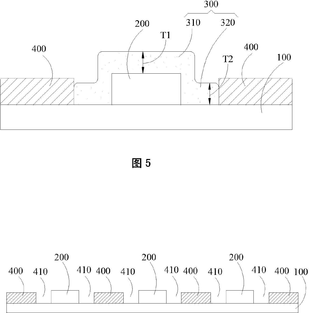
[0040] see image 3 , is a schematic diagram of the light-emitting device of the present invention. The present invention is a light emitting device, the light emitting device is a flat light emitting device, which includes: a substrate 100 , a light emitting diode chip 200 is arranged on the substrate 100 , and a phosphor layer 300 covers the light emitting diode chip 200 . Wherein the phosphor layer 300 has a first covering portion 310 and a second covering portion 320, the first covering portion 310 covers the top surface of the light emitting diode chip 200, the second covering portion 320 is located at the periphery of the light emitting diode chip 200 The top surface of the second cov...


PUM


Abstract

The invention relates to a light-emitting device, in particular to the structural improvement of a phosphor layer on a light-emitting diode chip. The light-emitting device comprises a substrate, the light-emitting diode chip and the phosphor layer, wherein the phosphor layer is provided with a first covering part and a second covering part; the first covering part is positioned on the top surface of the light-emitting diode chip; the second covering part covers the surface of the substrate around the light-emitting diode chip; height difference is formed between the top surface of the second covering part and the top surface of the first covering part. By the structural improvement of the phosphor layer, the color temperature difference value between the middle area and the edge area of the light-emitting device is reduced, and the light-emitting device has relatively high light-emitting quality.

Description

technical field [0001] The invention relates to a light-emitting device, in particular to a structural improvement of a fluorescent powder layer on a light-emitting diode chip. Background technique [0002] Light-emitting diodes (LEDs) have the advantages of low power consumption, long life, fast response, and small size. At present, the global white LED lighting industry continues to flourish, especially in mobile phone panel backlight, lighting and automotive industries. potential. [0003] At present, white light emitting devices on the market are mainly divided into two mainstreams. The first is to use phosphor to convert the blue light or ultraviolet light generated by blue LED or ultraviolet UV-LED into two-wavelength (Dichromatic) or three-wavelength (Trichromatic) white light, this technology is called phosphor powder conversion white light LED (Phosphor Converted-LED); the second type is a multi-chip white LED, which combines two (or more) LEDs of different colors...

Claims


Application Information

Patent Timeline
IPC IPC(8): H01L33/50
CPCH01L33/505H01L2933/0041
Inventor 陈奉宽黄义杰陈律安
Owner GENIUS ELECTRONICS OPTICAL CO LTD
Why Eureka
Try Eureka