A kind of LED encapsulation structure and preparation method thereof
A technology for LED packaging and LED chips, applied in semiconductor devices, electrical components, circuits, etc., can solve problems such as affecting the life of LED packaging devices, low thermal conductivity of LED chips, and inability to effectively conduct phosphors, so as to improve spatial color temperature distribution, Improve light conversion efficiency and solve the effect of thermal failure
- Summary
- Abstract
- Description
- Claims
- Application Information
AI Technical Summary
Problems solved by technology
Method used
Image

Examples
Embodiment 1
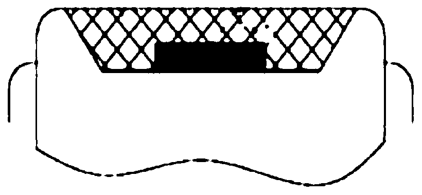
[0060] This embodiment discloses an LED packaging structure 1, such as Figure 5-11 As shown, it includes an LED chip 11 , an LED carrier 12 , a light conversion layer 13 and an outer protective layer 14 , and the LED chip 11 is disposed on the LED carrier 12 .
[0061] The LED packaging structure 1 also includes a transparent silicone layer 15 , which is wrapped between the light conversion layer 13 and the LED chip 11 , and the transparent silicone layer 15 becomes a supporting platform for the light conversion layer 13 .
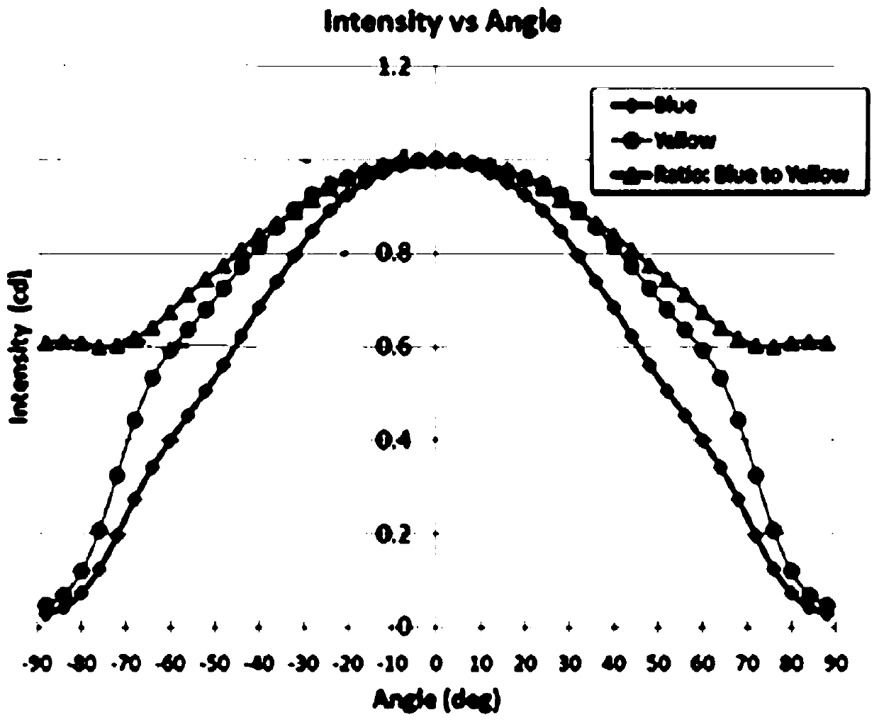
[0062] The thickness of the light conversion layer 13 located above the transparent silica gel layer 15 gradually decreases from the central area to the surrounding area, that is, this part of the light conversion layer 13 forms a structure that is thick in the center and thin in the periphery. The light conversion layer 13 located on the side wall of the transparent silica gel layer 15 The thickness gradually increases from top to bottom, which effective...
Embodiment 2
[0081]This embodiment discloses another LED packaging structure 2, and its structural difference from the LED packaging structure 1 described in Embodiment 1 lies in:
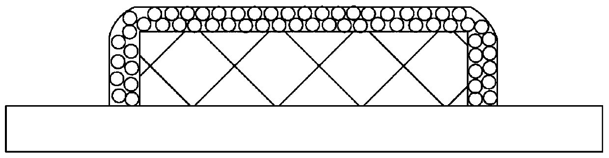
[0082] In this example, if Figures 14 to 17 As shown, according to the optical performance requirements, the surface of the fourth transparent silica gel layer 154 located above the LED chip 11 is concave downward and has a hemispherical shape, and the fifth transparent silica gel layer 155 located on the side wall of the LED chip 11 presents an outwardly flared slope. shape.
[0083] Based on the above-mentioned structural design, combined with the characteristics of the light conversion layer 13 as a fluid, the light conversion layer 13 located in the middle area above the LED chip 11 is also thicker, and the peripheral area is thinner. The light conversion layer located on the side of the LED chip 11 The thickness of 13 gradually increases from top to bottom, thereby effectively reducing the optical path d...
Embodiment 3
[0088] This embodiment discloses another LED package structure 3, which differs from the LED package structure 1 described in Embodiment 1 in terms of structure:
[0089] In this example, if Figures 19-22 As shown, the sixth transparent silica gel layer 156 located above the LED chip 11 is in the shape of a slope with high surroundings and a low middle, and the surface is X-shaped, and the seventh transparent silica gel layer 157 located on the side wall of the LED chip 11 is outwardly opened. Slope-like, similar to cutting two grooves along two diagonal lines on the surface of the transparent silicone layer 15 .
[0090] Based on the above-mentioned structural design, combined with the characteristics of the light conversion layer 13 as a fluid, the light conversion layer 13 located in the middle area above the LED chip 11 is also thicker, and the peripheral area is thinner. The light conversion layer located on the side of the LED chip 11 The thickness of 13 gradually incr...
PUM
 Abstract
Description
Claims
Application Information
 - R&D
- Intellectual Property
- Life Sciences
- Materials
- Tech Scout
- Unparalleled Data Quality
- Higher Quality Content
- 60% Fewer Hallucinations
Browse by: Latest US Patents, China's latest patents, Technical Efficacy Thesaurus, Application Domain, Technology Topic, Popular Technical Reports.
© 2025 PatSnap. All rights reserved.Legal|Privacy policy|Modern Slavery Act Transparency Statement|Sitemap|About US| Contact US: help@patsnap.com