Silicon wafer grinding device used for silicon wafer treatment

A technology for grinding wafers and silicon wafers, applied in the field of solar wafer manufacturing, can solve the problems of low safety and reliability, low processing efficiency, re-damage of silicon wafers, etc., so as to improve the qualified rate, facilitate the combination, and reduce the proportion of unqualified wafers. Effect

Inactive Publication Date: 2014-06-25
KONCA SOLAR CELL
View PDF7 Cites 2 Cited by
  • Summary
  • Abstract
  • Description
  • Claims
  • Application Information

AI Technical Summary

Problems solved by technology

The traditional treatment method is to manually polish the edge of the silicon wafer with sand paper. This method has the disadvantages of low processing efficiency, easy damage to the silicon wafer, and low safety and reliability.

Method used


Image

  • Silicon wafer grinding device used for silicon wafer treatment

Examples


Embodiment Construction

[0015] The technical solutions of the present invention will be further described below in conjunction with the accompanying drawings and through specific implementation methods.

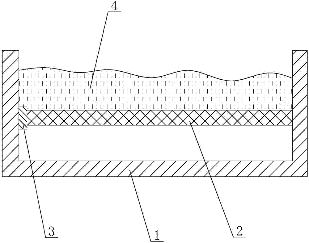
[0016] see figure 1 as shown, figure 1 It is a schematic structural diagram of a polishing device for silicon wafer processing provided in Embodiment 1 of the present invention.

[0017] In this embodiment, a wafer grinding device for processing silicon wafers includes a box body 1 with one end open, and the box body 1 is made of foam plastic, and its specifications are: length 582 mm, height 117 mm, depth 70 mm. And the box body 1 is fixed with a double-sided frosted glass 2 for polishing the silicon wafer. On the inner wall of the box body 1. The arrangement of the spacer 3 is used to prevent friction between the double-sided frosted glass 2 and the inner wall of the box body 1 during grinding. And the box body 1 contains a mortar 4 above the double-sided frosted glass 2, and the mortar 4 is f...


PUM


Abstract

The invention discloses a silicon wafer grinding device used for silicon wafer treatment. The silicon wafer grinding device comprises a plastic box with an opening in one end, a grinding piece used for grinding a silicon wafer is fixed in the plastic box, and space, above the grinding piece, in the plastic box is filled with mortar. Because the box of the silicon wafer grinding device for silicon wafer treatment is made of light plastic, the silicon wafer grinding device has the advantages of being detachable, capable of being cleaned a plurality of times, convenient to combine and use, safe and reliable, successfully treating silicon wafer edges in a batch mode, improving machined silicon wafer yield, shortening the time for treating silicon wafers with defective edges, and reducing the proportion of unqualified silicon wafers in the production process.

Description

technical field [0001] The invention belongs to the solar silicon chip manufacturing technology, in particular to a chip grinding device for processing unqualified chipped silicon chips into qualified chips. Background technique [0002] In the production process of solar silicon wafers, after the glue is removed, the adhesive surface of the silicon wafers at the two ends of the silicon wafers presents shiny edges, and the shiny edges of the silicon wafers are chipping. There are many reasons for the edge chipping of silicon wafers, and it is difficult to solve them all in actual production control. Every time silicon wafers are cut by wire, 1.8%-2% of unqualified chipped silicon wafers will occur. Accounted for 38% of unqualified films. The traditional treatment method is to manually polish the edge of the silicon wafer with sand paper. This method has the disadvantages of low processing efficiency, easy damage to the silicon wafer, and low safety and reliability. Conten...

Claims


Application Information

Patent Timeline
Patent Type & Authority Applications(China)
IPC IPC(8): B24B9/06
CPCB24B9/065
Inventor 宋吉袁琦杨乐
Owner KONCA SOLAR CELL
Why Eureka
Try Eureka