Supercharge Your Innovation With Domain-Expert AI Agents!

Method of depositing film

A film-forming method and technology of a film-forming device, which are applied in the directions of gaseous chemical plating, coating, electrical components, etc., can solve problems such as inability to properly adsorb, film wafers, etc.

Active Publication Date: 2014-06-25
TOKYO ELECTRON LTD
View PDF7 Cites 1 Cited by
  • Summary
  • Abstract
  • Description
  • Claims
  • Application Information

AI Technical Summary

Problems solved by technology

[0007] After that, in order to form an aluminum oxide (AlO) film in the above-mentioned laminated structure, the reaction gas A is set to trimethylaluminum (TMA) gas, which is an Al-containing organometallic gas, and the reaction gas B is set to O 3 When the film-forming process is carried out with the gas, there is a problem that the TMA gas is not adsorbed on the wafer on which only the TEMAZ gas is adsorbed, resulting in a wafer that cannot be formed into a laminated structure.
That is, in the film formation process, there is a characteristic that the raw material gases cannot be properly adsorbed when they are in direct contact with each other. In the above film formation process, there is a problem that such wafers are produced

Method used


Image

  • Method of depositing film
  • Method of depositing film
  • Method of depositing film

Examples


Embodiment approach 1

[0032] Film forming device

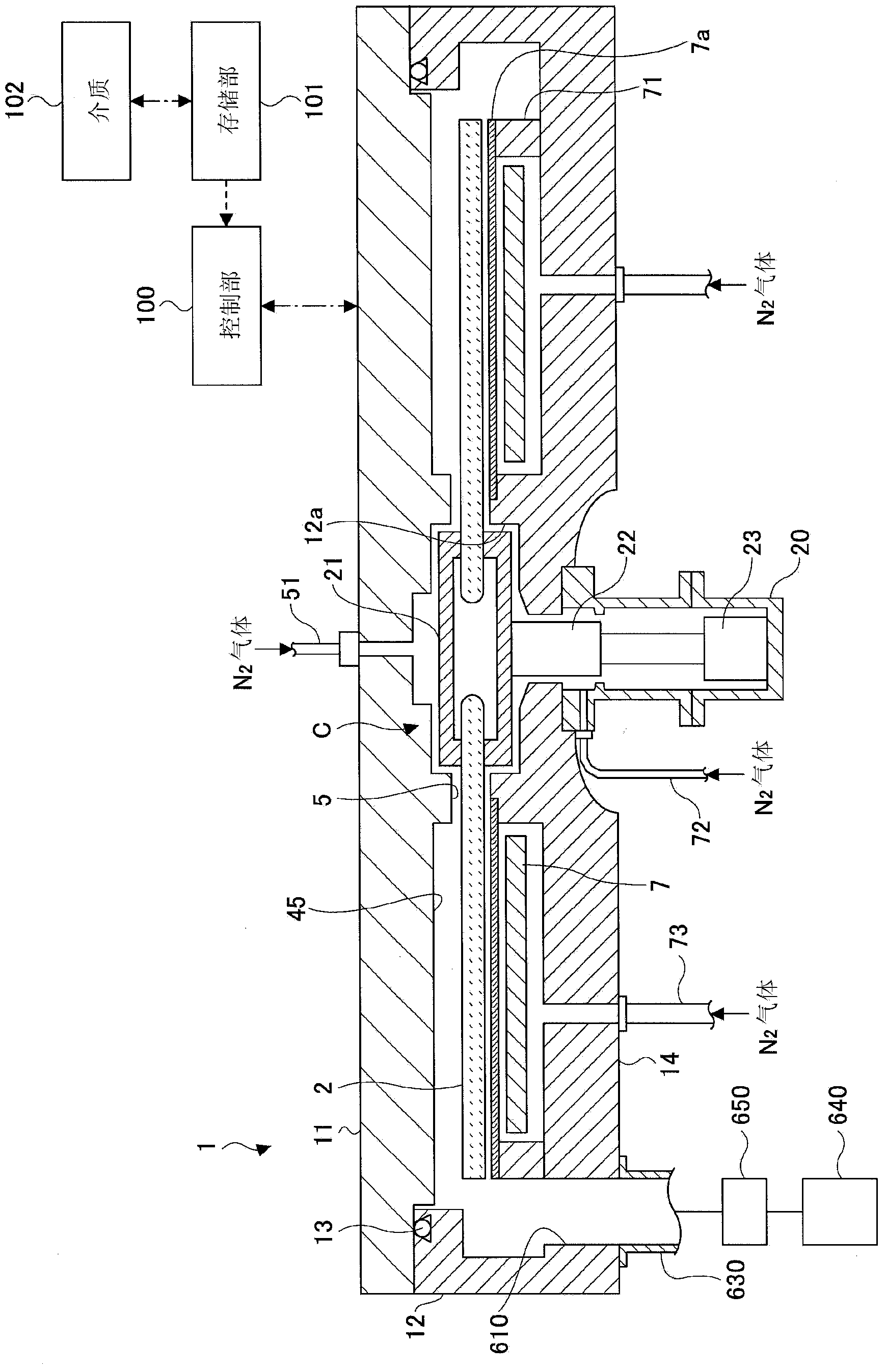
[0033] First, use Figure 1 ~ Figure 3 A film forming apparatus suitable for carrying out the film forming method according to Embodiment 1 of the present invention will be described.

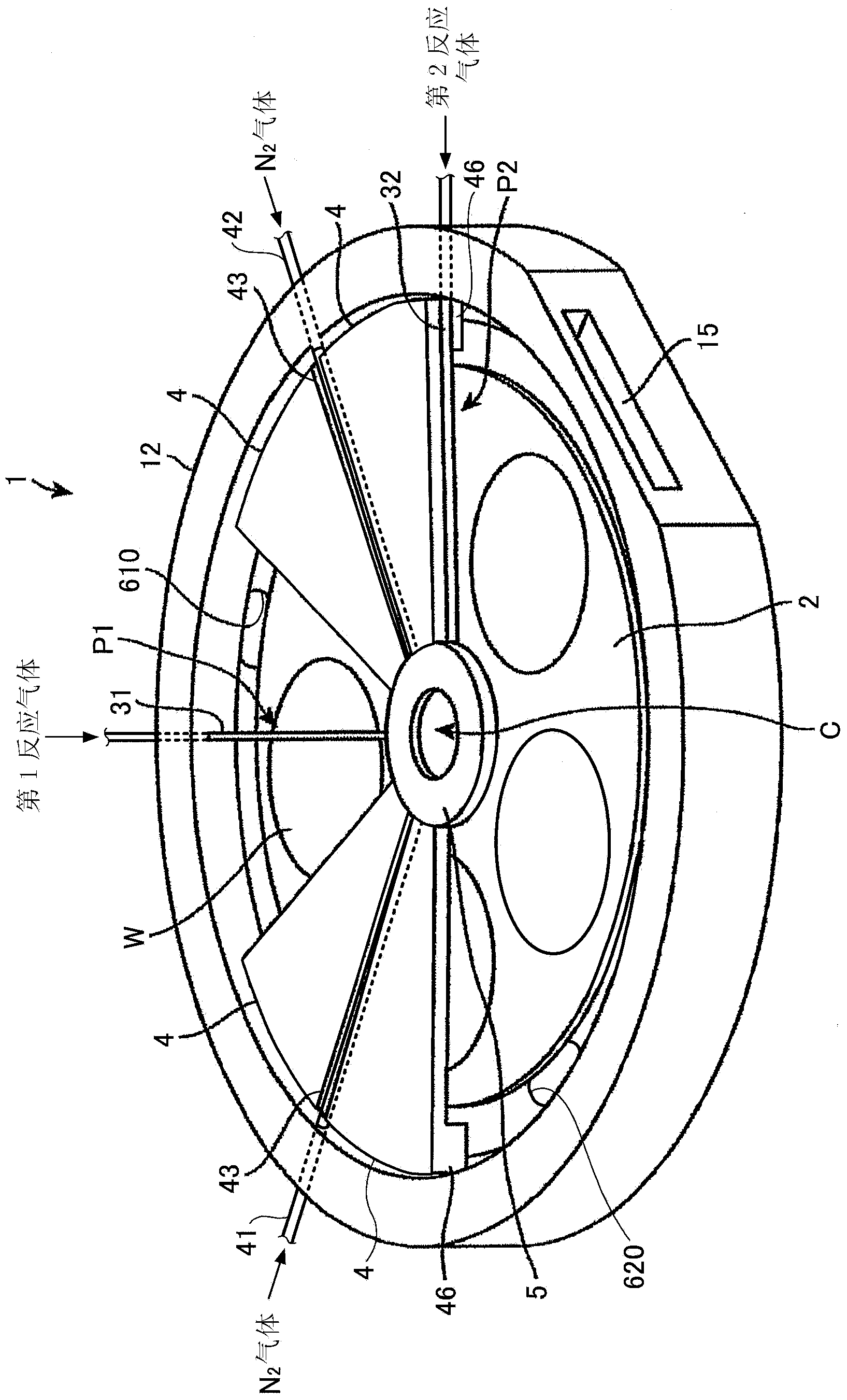
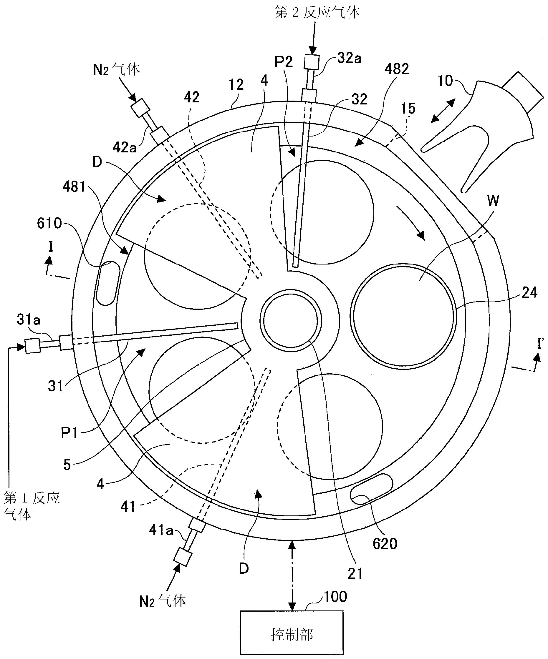
[0034] figure 1 It is a cross-sectional view showing a film forming apparatus suitable for carrying out the film forming method according to the embodiment of the present invention. figure 2 yes means figure 1 A perspective view of the structure inside the vacuum vessel of the film formation apparatus. image 3 yes means figure 1 A schematic plan view of the structure inside the vacuum chamber of the film formation apparatus.

[0035] refer to Figure 1 to Figure 3 , The film forming apparatus of Embodiment 1 includes: a flat chamber 1 having a substantially circular planar shape; The chamber 1 has: a container main body 12 having a bottomed cylindrical shape; a top plate 11 sandwiching a sealing member 13 such as an O-ring ( figure 1 ) is airtightly and ...

Embodiment approach 2

[0100] Figure 8 It is a sequence diagram showing an example of the film forming method according to Embodiment 2 of the present invention. In the film formation method of Embodiment 2, it is explained that the hafnium oxide (HfO) film and silicon oxide (collectively referred to as "SiO") may contain SiO 2 ) film formed as an example of an HfSiO film in a laminated configuration. The HfSiO film is also used as a so-called High-k film having a high dielectric constant.

[0101] In addition, in Embodiment 2, an example in which the same film-forming apparatus as that described in Embodiment 1 is used as the film-forming apparatus will be described. In addition, descriptions of the same contents as in Embodiment 1 are omitted or simplified as appropriate.

[0102] exist Figure 8 In step 1, a standby process is performed. In addition, since the content of introducing the wafer W into the chamber 1 until entering the standby process is the same as that described in Embodiment...

Embodiment approach 3

[0124] Figure 10 It is a figure which shows an example of the sequence of the film-forming method of Embodiment 3 of this invention. In Embodiments 1 and 2, an example of forming an oxide film was given and described, but in Embodiment 3, an example of forming a nitride film will be described. Specifically, in the film-forming method of Embodiment 3, film-forming of a TiAlN film having a laminated structure composed of a TiN film and an AlN film will be described as an example. In addition, a TiAlN film is also used as a so-called High-k film having a high dielectric constant.

[0125] In addition, in Embodiment 3, an example in which the same film formation apparatus as that described in Embodiments 1 and 2 is used as the film formation apparatus will be described. In addition, descriptions of the same contents as those in Embodiments 1 and 2 are appropriately omitted or simplified.

[0126] exist Figure 10 In the same manner as Embodiments 1 and 2, the turntable 2, the...


PUM


Abstract

The invention provides a method of depositing a film by means of a depositing device. The depositing device comprises a first air supply part, a second air supply part and a turntable used for loading a plurality of substrates. The method of depositing the film comprises a first step, a second step, a third step and a fourth step. During the first step, an oxidation air is supplied to rotate the turntable by means of the first and second air supply parts. During the second step, a first reaction air containing a first element is supplied by the first air supply part, and the oxidation air is supplied by the second air supply part so as to rotate the turntable. In this way, a first oxide film containing the first element is formed on a substrate. During the third step, the oxidation air is supplied to rotate the turntable by means of the first and second air supply parts. During the fourth step, a second reaction air containing a second element is supplied by the first air supply part and the oxidation air is supplied by the second air supply part so as to rotate the turntable. In this way, a second oxide film containing the second element is formed on the substrate.

Description

technical field [0001] The present invention relates to a film forming method, in particular to a film forming method for forming an oxide film or a nitride film containing a predetermined first element and a second element. Background technique [0002] In the manufacturing process of a semiconductor integrated circuit (IC: Integrated Circuit), there is a process of forming a thin film on a semiconductor wafer. In this process, from the viewpoint of further miniaturization of the IC, it is required to improve the uniformity of the thin film within the wafer surface. As a film-forming method that meets such demands, it is expected to employ a film-forming method called an atomic layer film deposition (ALD: Atomic Layer Deposition) method or a molecular layer film deposition (MLD: Molecular Layer Deposition) method. In the ALD method, one of the two reaction gases (reaction gas A) that reacts with each other is repeatedly adsorbed on the surface of the wafer and the other re...

Claims


Application Information

Patent Timeline
Patent Type & Authority Applications(China)
IPC IPC(8): C23C16/40C23C16/455
CPCH01L21/02189H01L21/02164H01L21/68771H01L21/02178H01L21/0228C23C16/00H01L21/02148H01L21/022C23C16/4584C23C16/45551H01L21/68764H01L21/02194
Inventor 池川宽晃上西雅彦高桥宏辅小堆正人小川淳
Owner TOKYO ELECTRON LTD
Features
  • R&D
  • Intellectual Property
  • Life Sciences
  • Materials
  • Tech Scout
  • Unparalleled Data Quality
  • Higher Quality Content
  • 60% Fewer Hallucinations
Learn More