
Wiring method for double-face printed circuit board

A technology of double-sided printing and wiring method, which is applied in the direction of printed circuit parts, printed circuits connected with non-printed electrical components, etc. question

Inactive Publication Date: 2014-06-25
SHENZHEN GONGJIN ELECTRONICS CO LTD
View PDF4 Cites 1 Cited by
  • Summary
  • Abstract
  • Description
  • Claims
  • Application Information

AI Technical Summary

Problems solved by technology

[0003] The traditional double-sided printed circuit board is used for wiring on both the front and back sides, making it difficult to form a complete plane on the printed circuit board, which will lead to the problem that the electromagnetic compatibility (EMC) cannot meet the requirements

Method used


Image

  • Wiring method for double-face printed circuit board
  • Wiring method for double-face printed circuit board

Examples


Embodiment Construction

[0013] In order to make the objectives, features, and advantages of the present invention more obvious and understandable, the specific embodiments of the present invention will be described in detail below with reference to the accompanying drawings. It should be pointed out that the terms related to the orientation in the present invention, such as "front", "back", "left", "right", etc., do not limit the orientation of the product when it is in use or other states, but merely indicate The relative position of the components in space.

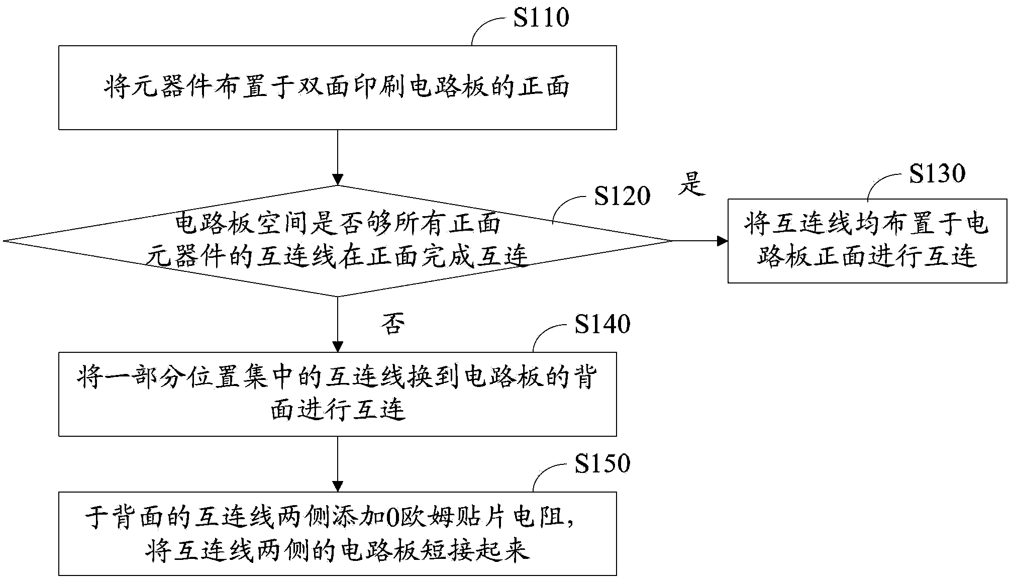
[0014] figure 1 It is a flowchart of the wiring method of a double-sided printed circuit board in an embodiment, including the following steps:

[0015] S110, arrange the components on the front side of the double-sided printed circuit board.

[0016] If the front space is not enough to place all the components, some components can also be placed on the back of the double-sided printed circuit board, and the components on the back should be concentr...


PUM


Abstract

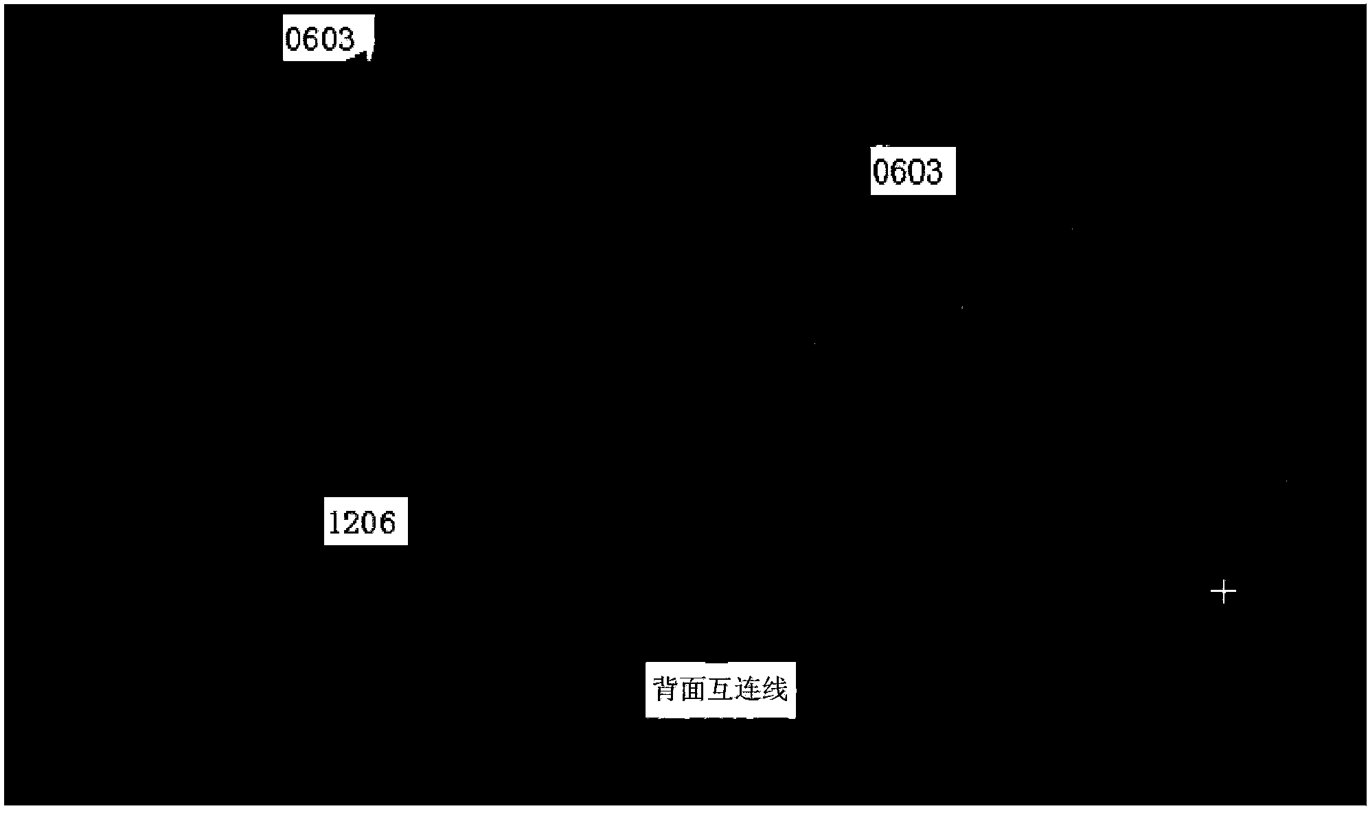
The invention relates to a wiring method for a double-face printed circuit board. The wiring method comprises steps that: components are arranged at a front face of the double-face printed circuit board; whether the circuit space is enough for mutual connection of mutual connection wires of the components at the front face is determined, if yes, all the mutual connection wires are arranged at the top layer for mutual connection; if not, the partial mutual connection wires which are concentrated at a position are shifted to a back face of the circuit board for mutual connection; two sides of the mutual connection wires at the back face are added with zero Ohm paster resistors, and the circuit boards at two sides of the mutual connection wires are in short connection. According to the wiring method, concentrated layer change of the mutual connection wires needing layer change is carried out, so a relatively-large-area complete plane is acquired at the back face of the double-face printed circuit board, the two zero Ohm resistors are utilized to complete the plane at two sides of the mutual connection wires, the risk of EMC rejection is greatly reduced, the passing percent of three Cs of products and CE authentication is greatly improved by employing the double-face printed circuit board, a reject rate of the products is reduced, and the product market launch speed is effectively improved.

Description

Technical field [0001] The invention relates to a method for manufacturing a printed circuit, in particular to a wiring method for a double-sided printed circuit board. Background technique [0002] In order to reduce the cost of current electronic products, more and more products use double-sided printed circuit boards for circuit design, that is, the front side (top layer) and back side (bottom layer) of the printed circuit board will be used for wiring. Reduce to 2 layers. [0003] Traditional double-sided printed circuit boards are used for wiring on both the front and back sides, making it difficult to form a complete plane on the printed circuit board, which will cause the problem of electromagnetic compatibility (EMC) not meeting the requirements. Summary of the invention [0004] Based on this, it is necessary to provide a wiring method for a double-sided printed circuit board, which can manufacture a double-sided printed circuit board with good electromagnetic compatibilit...

Claims


Application Information

Patent Timeline
IPC IPC(8): H05K1/02H05K1/18
Inventor 王达国
Owner SHENZHEN GONGJIN ELECTRONICS CO LTD
Learn More