Silicon slice ejection mechanism

A silicon wafer and ejector pin technology, which is used in photolithography process exposure devices, microlithography exposure equipment, etc., can solve problems such as silicon wafer slippage, and achieve the effect of ensuring effective adsorption and improving motion control accuracy.

Active Publication Date: 2014-07-02
SHANGHAI MICRO ELECTRONICS EQUIP (GRP) CO LTD +1
View PDF6 Cites 6 Cited by
  • Summary
  • Abstract
  • Description
  • Claims
  • Application Information

AI Technical Summary

Problems solved by technology

[0004] The invention provides a silicon chip pushing mechanism to overcome the silicon chip slipping problem caused by the inability of the warped and ultra-thin chips to be completely absorbed in the prior art

Method used


Image

  • Silicon slice ejection mechanism
  • Silicon slice ejection mechanism
  • Silicon slice ejection mechanism

Examples


Embodiment Construction

[0025] In order to make the above objects, features and advantages of the present invention more comprehensible, specific implementations of the present invention will be described in detail below in conjunction with the accompanying drawings. It should be noted that all the drawings of the present invention are in simplified form and use inaccurate scales, and are only used to facilitate and clearly assist the purpose of illustrating the embodiments of the present invention.

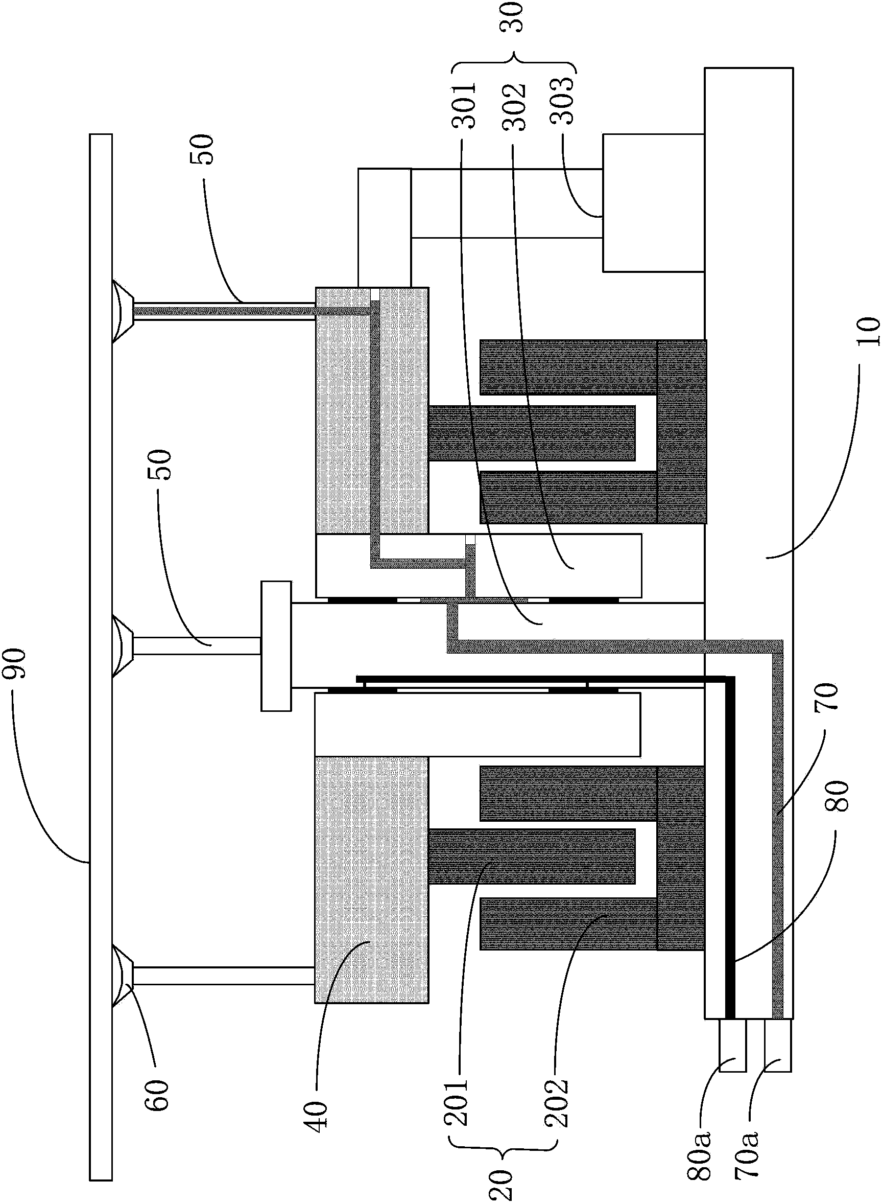
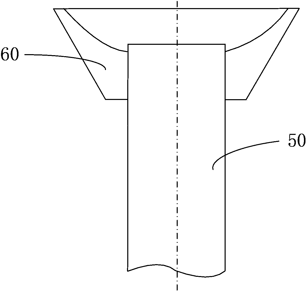
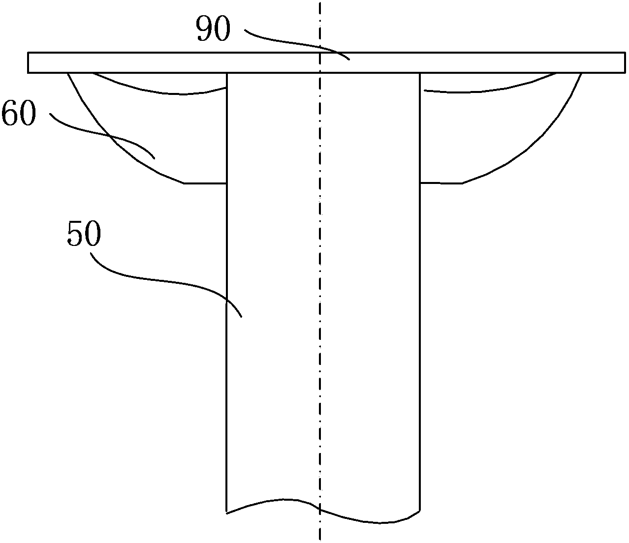
[0026] Please refer to figure 1 , and combined with Figure 2~4 , the present invention provides a silicon wafer ejection mechanism, comprising: a base 10, a driving mechanism 20, a guide mechanism 30, a connecting plate 40 and an ejection pin 50, the driving mechanism 20 is fixed on the base 10, the The pushing pin 50 and the guide mechanism 30 are fixed on the connecting plate 40 . Preferably, the wafer pushing mechanism further includes a flexible suction cup 60 , the flexible suction cup 60 is arr...


PUM


Abstract

The invention discloses a silicon slice ejection mechanism, comprising a base, a drive mechanism, a guide mechanism, a connection plate and an ejection pin, wherein the drive mechanism is fixed on the base; the ejection pin and the guide mechanism are fixed on the connection plate; the silicon slice ejection mechanism also comprises a flexible suction plate; the flexible suction plate is arranged at the top of the ejection pin and connected with the ejection pin; and the connection height of the inner side of the flexible suction plate is smaller than the height of the top surface of the ejection pin. The flexible suction plate is additionally arranged at the top of the ejection pin; compared with a nonmetallic material in the prior art, the flexible suction plate is softer and can be in tight fit with a warping sheet and an ultra-thin sheet to achieve a vacuum and leak-proof effect, and thus the effective adsorption of the silicon slice is ensured.

Description

technical field [0001] The invention relates to the field of photolithography equipment manufacturing, in particular to a silicon wafer pushing mechanism. Background technique [0002] With the development of the semiconductor industry, more and more advanced technologies have been applied to this industry. Existing lithography devices are generally divided into two categories, one is a stepper lithography device, and the mask pattern is imaged on one exposure area of ​​the lens in one exposure; the other is a step-and-scan lithography device, and the mask pattern is not Instead of imaging with a single exposure, it is imaged through a scanning movement of the projected light field. In a step-and-scan lithography device, the workpiece table mainly includes a coarse motion table, a micro motion table and a push-out mechanism. Among them, the ejecting mechanism cooperates with the silicon wafer transmission system to complete the handover function of the silicon wafer. The ...

Claims


Application Information

Patent Timeline
Patent Type & Authority Applications(China)
IPC IPC(8): G03F7/20
Inventor 夏海王鑫鑫
Owner SHANGHAI MICRO ELECTRONICS EQUIP (GRP) CO LTD
Why Eureka
Try Eureka