A chip pick-and-place device

A pick-and-place device and chip technology, which is applied in transportation and packaging, semiconductor devices, electrical components, etc., can solve the problems of low pick-up accuracy, and achieve the effects of reducing axial installation accuracy requirements, high efficiency, and fast response speed

Active Publication Date: 2016-08-31
HUAZHONG UNIV OF SCI & TECH
View PDF8 Cites 0 Cited by
  • Summary
  • Abstract
  • Description
  • Claims
  • Application Information

AI Technical Summary

Problems solved by technology

The speed and precision of the chip pick-and-place device are mutually restricted. In multi-nozzle placement equipment, the fewer pick-up stations, the slower the running speed and the smaller the vibration, the higher the pick-up accuracy will be; the more pick-up stations, the higher the pick-up accuracy. The faster the speed, the lower the picking accuracy will be

Method used


Image

  • A chip pick-and-place device
  • A chip pick-and-place device
  • A chip pick-and-place device

Examples


Embodiment Construction

[0040] In order to make the object, technical solution and advantages of the present invention clearer, the present invention will be further described in detail below in conjunction with the accompanying drawings and embodiments. It should be understood that the specific embodiments described here are only used to explain the present invention, not to limit the present invention. In addition, the technical features involved in the various embodiments of the present invention described below can be combined with each other as long as they do not constitute a conflict with each other.

[0041] Now illustrate the present invention in conjunction with the preferred embodiment of accompanying drawing.

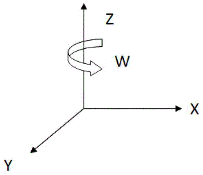
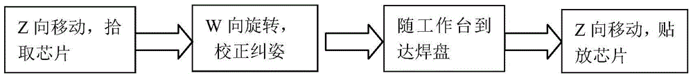
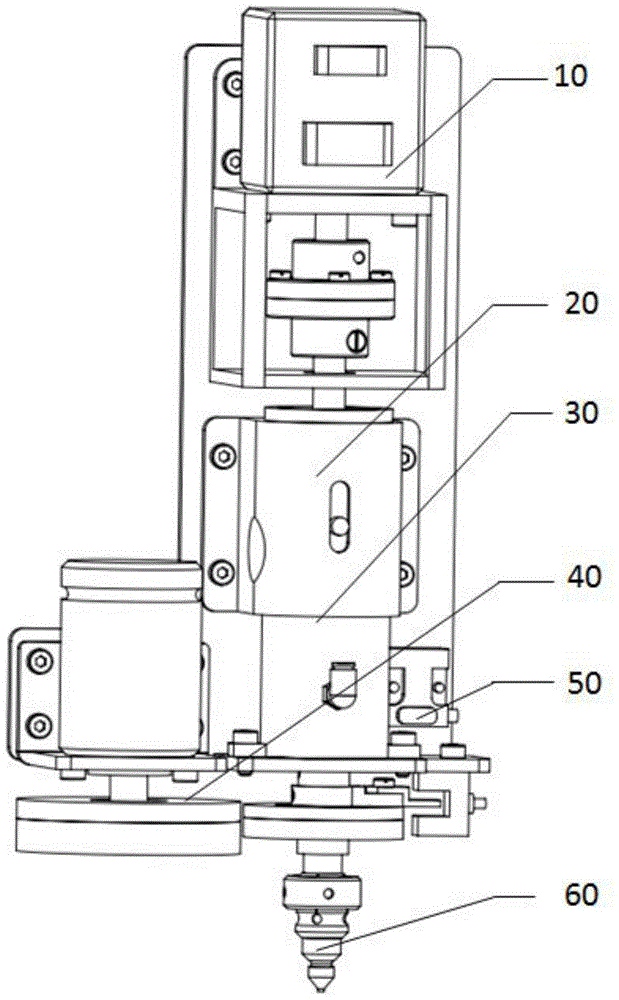
[0042] Such as image 3 As shown, the chip pick-and-place device of the present invention mainly includes a Z-direction drive assembly 10, a cam transmission assembly 20, an air gap bearing 30, a W rotation drive assembly 40, an air buffer assembly 50, and a chip adsorption assemb...


PUM


Abstract

The invention provides a chip picking and placing device which comprises a chip adsorbing component, a cam transmission component, a Z-direction driving component, an air gap bearing, an air buffering component and a W-direction rotation driving component, wherein the cam transmission component comprises a cam lever and a cam which are connected, the Z-direction driving component is connected with the upper end of the cam lever and used for driving the chip adsorbing component fixed inside the cam to move vertically along the Z axis, the air buffering component is installed inside the cam and used for absorbing the impact force borne by the chip adsorbing component, the W-direction rotation driving component is connected to the lateral side of the chip adsorbing component and used for driving the chip adsorbing component to rotate in the W direction, the air gap bearing is located outside the chip adsorbing component and arranged at the lower end of the air buffering component in a sleeved mode, and the inner ring of the bearing is suspended by introducing air into the space between the inner ring and outer ring of the air gap bearing so that the chip adsorbing component can be assisted in rotation in the W direction. The device is simple and compact in structure, high in production efficiency and yield, long in service life, and high in working reliability.

Description

technical field [0001] The invention relates to a chip pick-and-place device, in particular to a chip pick-up, transfer and placement device in the chip packaging process. Background technique [0002] Radio Frequency Identification (RFID, Radio Frequency Identification), also known as electronic tags and radio frequency identification, is a communication technology that can identify specific targets through radio signals and read and write related data without the need for mechanical or physical identification between the identification system and specific targets. optical contact. In the 21st century, it is an information technology with the most promising and application prospects. [0003] RFID label INLAY production equipment usually includes five modules: substrate conveying, dispensing, mounting, hot pressing and testing. The function of the mounting process is to ensure the precise alignment of the chip and the antenna, which is an indispensable and important link. ...

Claims


Application Information

Patent Timeline
Patent Type & Authority Patents(China)
IPC IPC(8): H01L21/677H01L21/683
CPCH01L21/6838H01L2221/683
Inventor 陈建魁尹周平王冠付宇
Owner HUAZHONG UNIV OF SCI & TECH
Why Eureka
Try Eureka