A kind of circuit board manufacturing process and circuit board

A circuit board manufacturing and process technology, applied in the directions of printed circuit manufacturing, printed circuits, printed circuit components, etc., can solve the problems of poor alignment accuracy, large thickness of copper foil, difference in impedance between surface and inner layers, etc. The effect of low alignment accuracy, reduction of repeated accumulation, and reduction of line width differences

Active Publication Date: 2017-08-29
LENOVO (BEIJING) LTD
View PDF4 Cites 0 Cited by
  • Summary
  • Abstract
  • Description
  • Claims
  • Application Information

AI Technical Summary

Problems solved by technology

[0004] The existing circuit board manufacturing process has at least the following defects: the step of further copper plating on the surface layer will cause the copper thickness around the lead hole to be larger than the copper foil thickness in the inner layer board, resulting in a gap between the surface layer and the inner layer board after the circuit is etched. There will be different line widths, which will lead to the impedance difference between the surface layer and the inner layer board, thereby causing interference to the device impedance and voltage calculation on the PCB, and the manual alignment and pasting of the shielding film will appear Technical issues with poor bit precision

Method used


Image

  • A kind of circuit board manufacturing process and circuit board
  • A kind of circuit board manufacturing process and circuit board
  • A kind of circuit board manufacturing process and circuit board

Examples


Embodiment Construction

[0027] The following will clearly and completely describe the technical solutions in the embodiments of the present invention with reference to the accompanying drawings in the embodiments of the present invention. Obviously, the described embodiments are only some, not all, embodiments of the present invention. Based on the embodiments of the present invention, all other embodiments obtained by persons of ordinary skill in the art without creative efforts fall within the protection scope of the present invention.

[0028] The embodiment of the invention discloses a circuit board manufacturing process and a circuit board, so as to achieve the technical effect of reducing etching errors and improving the alignment accuracy of a shielding layer.

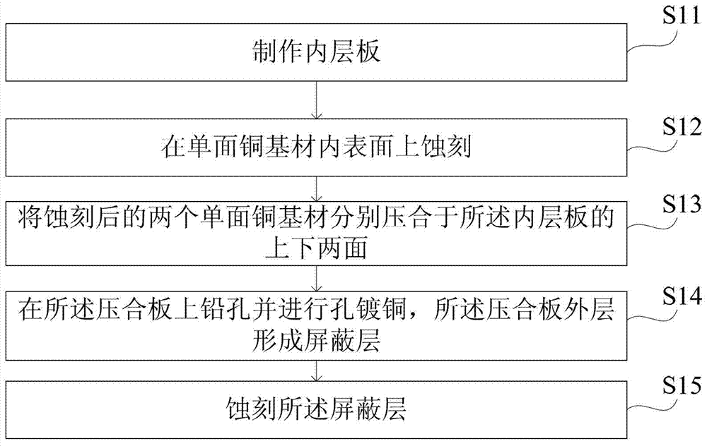
[0029] figure 1 A circuit board manufacturing process is shown, including:

[0030] S11: making the inner layer board;

[0031] The process for making the inner layer board can be composed of steps such as film application, exposure,...


PUM


Abstract

An embodiment of the invention discloses a process of manufacturing a circuit board and the circuit board. The process comprises making an inner plate; etching the inner surfaces of single-sided copper substrates, the outer surfaces of which comprises insulating layers; laminating the two etched single-sided copper substrates respectively onto the upper and lower sides of the inner plate to form a laminated board, with the inner surfaces of the etched single-sided copper substrate facing toward the inner plate and the non-etched insulating layers facing outward; drilling holes in the laminated board, conducting copper plating for the holes, and forming shielding layers outside the laminated board; and etching the shielding layers. The circuit board reduces the difference of line width between the surface layer and the inner plate after etching, and the technical problem of low alignment accuracy caused by manual alignment of the shielding layer in the prior art is solved.

Description

technical field [0001] The invention relates to the technical field of circuit board manufacturing, and more specifically, relates to a circuit board manufacturing process and a circuit board. Background technique [0002] The circuit board is the support of electronic components and the provider of electrical connections for electronic components. [0003] The existing circuit board manufacturing process is to perform mechanical lead holes on the inner layer board with the surface layer (copper foil) pressed together, and then perform copper plating on the hole and surface layer etching. In addition, in order to shield electromagnetic interference, after the circuit board is manufactured, the independent shielding film needs to be manually aligned and attached to the circuit board. [0004] The existing circuit board manufacturing process has at least the following defects: the step of further copper plating on the surface layer will cause the thickness of the copper aroun...

Claims


Application Information

Patent Timeline
Patent Type & Authority Patents(China)
IPC IPC(8): H05K3/00H05K1/02
Inventor 余秀青张笑为
Owner LENOVO (BEIJING) LTD
Why Eureka
Try Eureka