Phase shift mask and method of making the same, array substrate and method of making the same

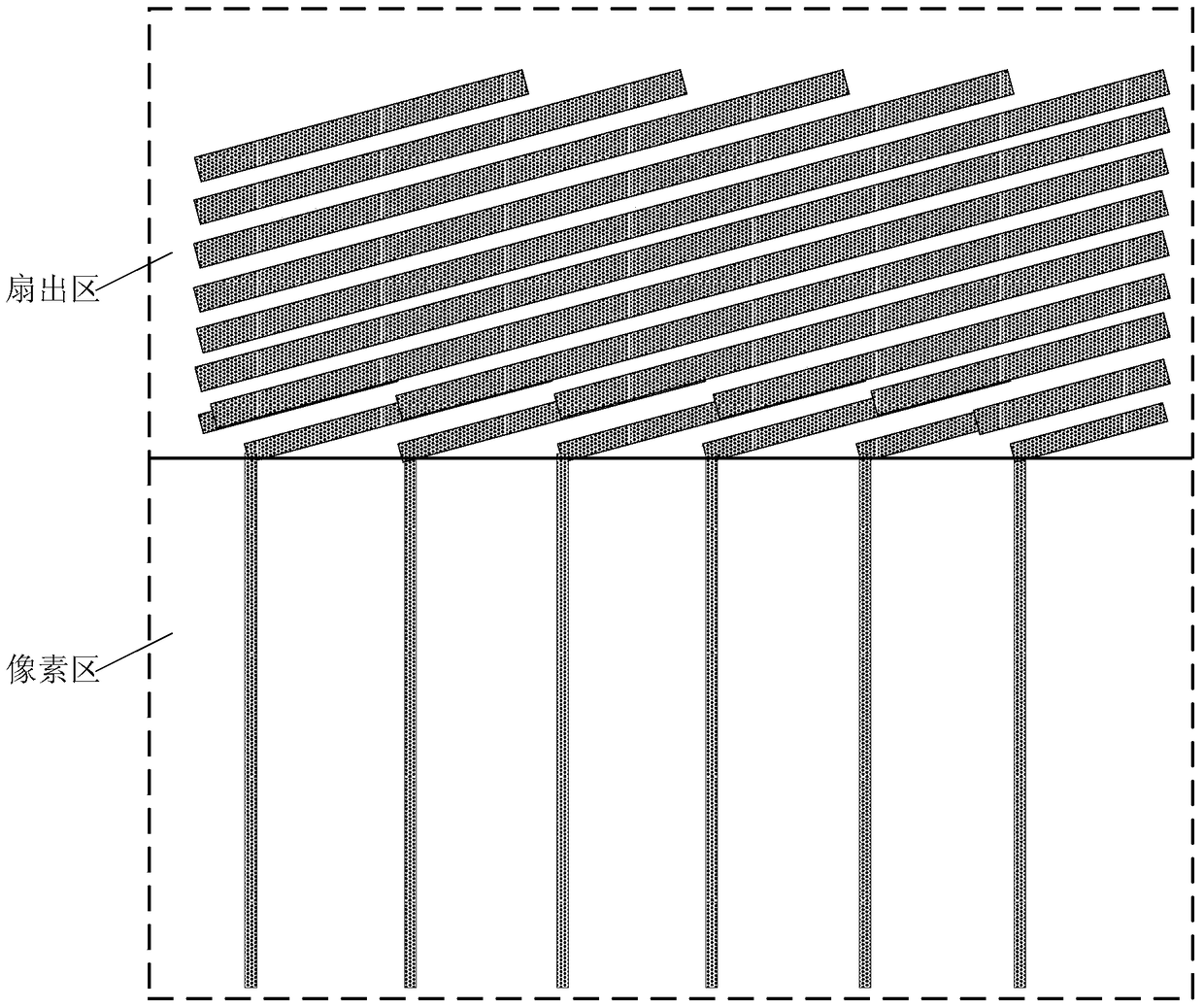
An array substrate and phase-shift mask technology, which is applied in the field of phase-shift mask and its manufacturing method, array substrate and its manufacturing, can solve the problem of dense signal lines in the fan-out area and sparse signal lines in the pixel area, etc. problem, achieve the effect of reducing the line width difference and reducing the difference

Active Publication Date: 2019-03-01
BOE TECH GRP CO LTD
View PDF11 Cites 0 Cited by
  • Summary
  • Abstract
  • Description
  • Claims
  • Application Information

AI Technical Summary

Problems solved by technology

The reasons for this defect are: (1) From the layout point of view, the signal lines in the pixel area are relatively sparse, while the signal lines in the fan-out area are relatively dense

Method used


Image

  • Phase shift mask and method of making the same, array substrate and method of making the same
  • Phase shift mask and method of making the same, array substrate and method of making the same
  • Phase shift mask and method of making the same, array substrate and method of making the same

Examples


Embodiment 1

[0082] The manufacturing method of the phase-shift mask plate of the present embodiment comprises the following steps:

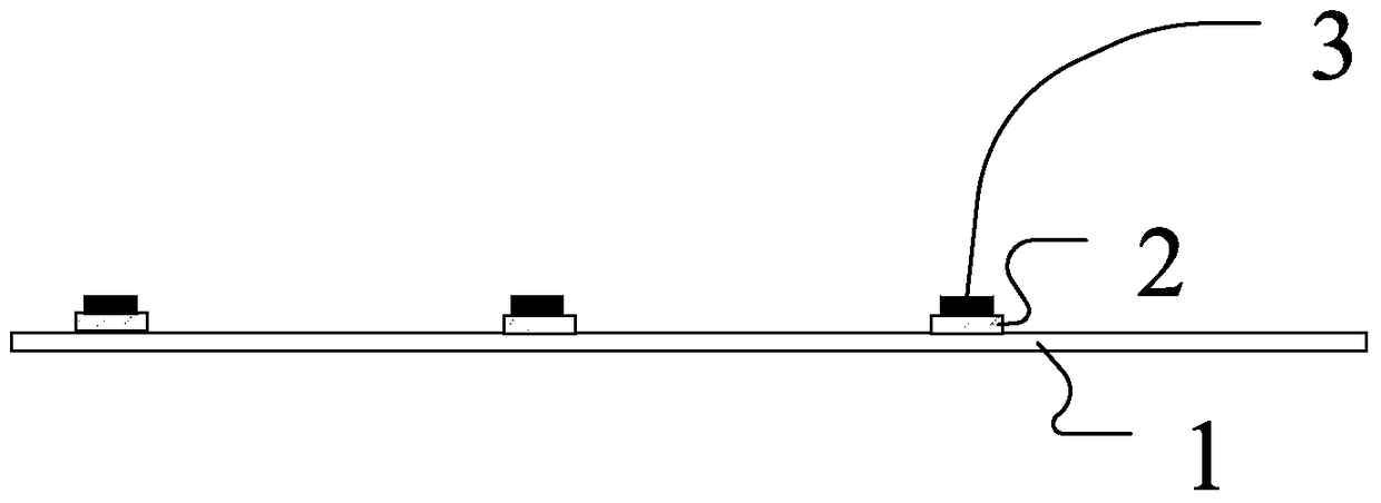
[0083] Step a1, such as Figure 8 As shown in (1), a substrate 1 is provided, and the substrate 1 may be a glass substrate or a quartz substrate. On the substrate 1, a phase shift layer 2 and an opaque layer 3 are sequentially formed, the material of the opaque layer 3 is chromium, and a photoresist 4 is coated on the opaque layer 3;

[0084] Step a2, such as Figure 8 As shown in (2), remove the photoresist outside the light-shielding pattern area after development, and etch the phase shift layer 2 and the light-impermeable layer 3 outside the light-shielding pattern area by dry etching;

[0085] Step a3, such as Figure 8 As shown in (3), the remaining opaque layer 3 is etched and thinned by a wet etching process;

[0086] Step a4, such as Figure 8 Shown in (4), remove remaining photoresist;

[0087] Step a5, such as Figure 8 Shown in (5), coat ph...

Embodiment 2

[0093] The manufacturing method of the phase-shift mask plate of the present embodiment comprises the following steps:

[0094] Step b1, such as Figure 8 As shown in (1), a substrate 1 is provided, and the substrate 1 may be a glass substrate or a quartz substrate. On the substrate 1, a phase shift layer 2 and an opaque layer 3 are sequentially formed, the material of the opaque layer 3 is chromium, and a photoresist 4 is coated on the opaque layer 3;

[0095] Step b2, such as Figure 8 As shown in (2), remove the photoresist outside the light-shielding pattern area after development, and etch the phase shift layer 2 and the light-impermeable layer 3 outside the light-shielding pattern area by dry etching;

[0096] Step b3, such as Figure 8As shown in (3), the remaining opaque layer 3 is etched and thinned by a wet etching process;

[0097] Step b4, such as Figure 8 Shown in (4), remove remaining photoresist;

[0098] Step b5, such as Figure 8 Shown in (5), coat pho...


PUM


Abstract

The invention provides a phase shifting mask and a manufacture method thereof, and an array substrate and a manufacture method thereof, and belongs to the field of display. The phase shifting mask is used for manufacturing signal lines of a pixel region and a fan-out region of the array substrate and comprises a plurality of shading patterns distributed in sequence and arranged in the one-to-one correspondence with the signal lines on the array substrate, wherein each shading pattern comprises first shading patterns at least corresponding to signal lines of the pixel region and second shading patterns except for the first shading lines; when the phase shifting mask is used for exposure, the light intensity received by photoresist below a first region between adjacent first shading patterns is smaller than the light intensity received by photoresist below a second region between adjacent second shading patterns. Through the adoption of the technical scheme, the line width difference between signal lines of the pixel region and signal lines of the fan-out region can be reduced.

Description

technical field [0001] The present invention relates to the display field, in particular to a phase-shift mask plate and a manufacturing method thereof, an array substrate and a manufacturing method thereof. Background technique [0002] Mask, also known as photomask or mask, is the link and bridge connecting the design end and the process manufacturing end. With the advancement of design technology and manufacturing process, a phase-shift mask has appeared. The phase-shift mask forms a pattern on the substrate and at the same time forms a phase-shift layer area and a non-phase-shift layer area. When using a phase-shift mask During the exposure process of the template, the light passing through the phase shift layer region will produce a 180° phase change, so as to better control the critical dimension (CD) of the pattern. [0003] One of the technology development trends of future flat panel display is the realization of high resolution. For this goal, edge phase shift mas...

Claims


Application Information

Patent Timeline
Patent Type & Authority Patents(China)
IPC IPC(8): G03F1/26
Inventor 黎午升
Owner BOE TECH GRP CO LTD
Why Eureka
Try Eureka