
Color film substrate, liquid crystal display panel and liquid crystal display device

A technology of liquid crystal display panels and color film substrates, applied in nonlinear optics, instruments, optics, etc., to achieve the effect of reducing color shift and improving color display effect

Active Publication Date: 2014-07-16
XIAMEN TIANMA MICRO ELECTRONICS +1
View PDF8 Cites 16 Cited by
  • Summary
  • Abstract
  • Description
  • Claims
  • Application Information

AI Technical Summary

Problems solved by technology

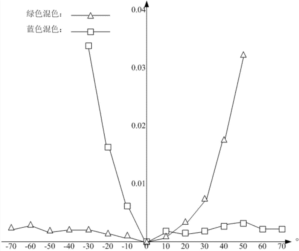
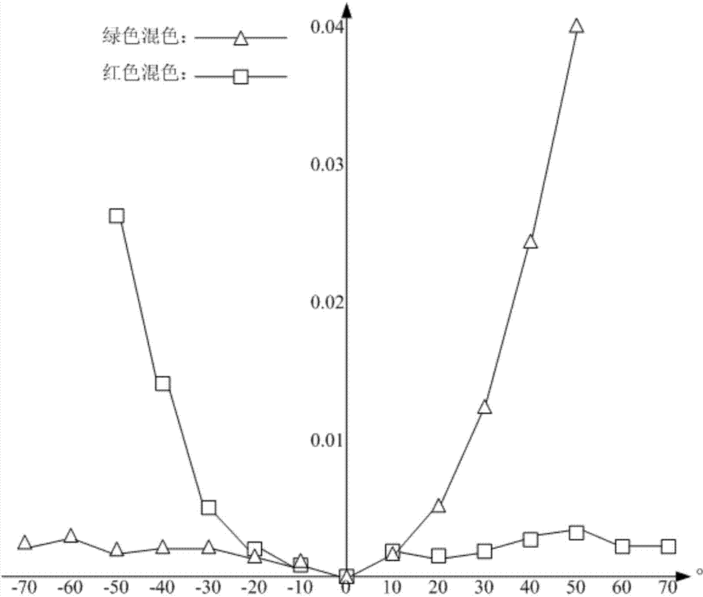
[0006] However, since the color shift caused by the mixing of blue in the green display screen and red in the green display screen is relatively light, it seems comprehensively that the mixing of red and blue is the most important color shift problem in the FFS mode LCD.

Method used


Image

  • Color film substrate, liquid crystal display panel and liquid crystal display device
  • Color film substrate, liquid crystal display panel and liquid crystal display device
  • Color film substrate, liquid crystal display panel and liquid crystal display device

Examples


Embodiment 1

[0028] image 3 It is a schematic diagram of the principle of reducing the color shift of the liquid crystal display device by increasing the width of the light-shielding layer according to Embodiment 1 of the present invention. see image 3 The liquid crystal display panel includes a TFT array substrate 330 , a color filter substrate 310 and a liquid crystal layer 320 disposed between them. The backlight source is disposed under the TFT array substrate 330 (not shown in the figure). The color filter substrate 310 includes a first color filter layer 311 , a second color filter layer 312 , and a light shielding layer 313 disposed between the first color filter layer 311 and the second color filter layer 312 . A data line 331 is disposed on the upper surface of the TFT array substrate 330 , and the data line 331 is disposed opposite to and parallel to the light shielding layer 313 .

[0029] When a driving voltage is applied to the TFT array unit facing the first color filter...

Embodiment 2

[0039] Figure 5It is a cross-sectional view of the color filter substrate provided in Embodiment 2 of the present invention. This embodiment is based on the above embodiments. Further, in the color filter substrate provided in this embodiment, the width of the first light-shielding layer 504 separating the red filter layer and the green filter layer is larger than that of the green filter layer. and the width of the second light-shielding layer 505 of the blue filter layer.

[0040] Since the intermixing between blue light and red light is the most serious, the intermixing between red light and green light is the second, and the intermixing between green light and blue light is the lightest, so the blue filter layer and the The width of the third shading layer of the red filter layer is the widest, the width of the first shading layer separating the red filter layer and the green filter layer is next, and the width of the first shading layer separating the green filter layer...

Embodiment 3

[0046] Figure 6 It is a schematic diagram of the principle of reducing the color shift of the liquid crystal display device by adjusting the position of the data line in Embodiment 3 of the present invention. see Figure 6 , the liquid crystal display panel includes a TFT array substrate 630 , a color filter substrate 610 and a liquid crystal layer 620 disposed between them. The color filter substrate 610 includes a first color filter layer 611 and a second color filter layer 612 . The light transmitted by the first color filter layer 611 is light with a first color, and the light transmitted by the second color filter layer 612 is light with a second color. A light shielding layer 613 is disposed between the first color filter layer 611 and the second color filter layer 612 . Data lines 631 are formed on the TFT array substrate 630 . The data line 631 is relatively parallel to the light-shielding layer.

[0047] When the TFT array unit disposed opposite to the first col...


PUM

PropertyMeasurementUnit
Widthaaaaaaaaaa
Widthaaaaaaaaaa
Widthaaaaaaaaaa

Abstract

The invention discloses a color film substrate, a liquid crystal display panel and a liquid crystal display device. The color film substrate comprises a red filter layer, a green filter layer, a blue filter layer, a first shade layer isolating the red and green filter layers, a second shade layer isolating the green and blue filter layers, and a third shade layer isolating the blue and red filter layers. The third shade layer is wider than the first and second shade layers. According to the embodiments, the shade layer between the blue and red filter layers is widened, color shift of the liquid crystal display panel is significantly decreased, and display effect of the liquid crystal display panel is improved.

Description

technical field [0001] The invention relates to the technical field of liquid crystal display, in particular to a color filter substrate, a liquid crystal display panel and a liquid crystal display device. Background technique [0002] In Thin Film Transistor Liquid Crystal Display (TFT-LCD) products, Fringe Field Switching (FFS) can improve the performance of In-Plane-Switching (IPS) mode liquid crystals. The aperture ratio and transmittance of the display. [0003] The liquid crystal display of FFS mode comprises common electrode and pixel electrode, and the distance between common electrode and pixel electrode can be controlled to be less than the distance between upper and lower glass substrates, so that fringe field can be formed between common electrode and pixel electrode, thus, It can control the liquid crystal molecules located above the pixel electrodes, overcome the defect that the electric field directly above the pixel electrodes of the traditional IPS liquid c...

Claims


Application Information

Patent Timeline
IPC IPC(8): G02F1/1335
Inventor 沈柏平吴玲张沼栋
Owner XIAMEN TIANMA MICRO ELECTRONICS
Learn More