Modulation driving output stage circuit

A technology for driving output and stage circuits, which is applied in the field of modulation and driving output stage circuits, which can solve the problem that the driver transistor cannot be switched quickly, and achieve the effects of fast switching, increasing voltage margin, and reducing voltage margin

Active Publication Date: 2014-07-30
JIAXING HEROIC ELECTRONICS TECH
View PDF5 Cites 1 Cited by
  • Summary
  • Abstract
  • Description
  • Claims
  • Application Information

AI Technical Summary

Problems solved by technology

[0006] In view of the above-mentioned defects of the prior art, the technical problem to be solved by the present invention is to provide a modulating drive output stage circuit, which can increase the voltage margin of the driver, so as to avoid the driver from causing insufficient margin when the power supply voltage is low. The problem of transistors not being able to switch quickly

Method used


Image

  • Modulation driving output stage circuit
  • Modulation driving output stage circuit

Examples


Embodiment Construction

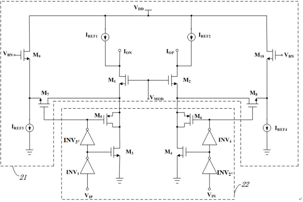
[0017] Such as figure 2 Shown is a modulation drive output stage circuit of a preferred embodiment of the present invention, which is a symmetrical circuit on the left and right sides. The modulation drive output stage circuit includes a switch control circuit section 22 and a current generation circuit section 21 . The switch control circuit section 22 receives a differential input voltage (V IP , V IN ), where the differential input voltage comprises the first differential voltage V IP and the second differential voltage V IN . The current generation circuit part 21 is connected to the switch control circuit part 22, and outputs a differential output current (I OP , I ON ), where the differential input voltage includes the first differential current I OP and the second differential current I ON .

[0018] In an embodiment of the present invention, the current generating circuit part 21 includes a first transistor M 1 , the second transistor M 2 , the seventh tran...


PUM


Abstract

The invention provides a modulation driving output stage circuit. The modulation driving output stage circuit comprises a switch control circuit part and a current generation circuit part. The modulation driving output stage circuit receives a pair of difference input voltages and outputs a pair of difference output currents. The current generation circuit part comprises a first transistor, a second transistor, a first reference current source and a second reference current source. The switch control circuit part comprises a third transistor, a fourth transistor, a first phase inverter and a second inverter. The first difference voltage in the pair of difference input voltages is input into the grid electrode of the third transistor through the first phase inverter, the second difference voltage in the pair of difference input voltages is input into the grid electrode of the fourth transistor through the second phase inverter, the drain electrode of the second transistor outputs the first difference current in the pair of difference output currents, and the drain electrode of the first transistor outputs the second difference current in the pair of difference output currents. The modulation driving output stage circuit can increase the voltage margin of a driver.

Description

technical field [0001] The invention relates to a modulation driving circuit, in particular to a modulation driving output stage circuit applied in a laser driver. Background technique [0002] With the advancement of science and technology, optical fiber communication has entered various fields of wired communication and has become the mainstream of communication development. To realize optical fiber network communication, the first problem to be solved is how to load the signal to the optical fiber channel, that is, optical modulation is required. [0003] The simplest and most widely used modulation strategy is on-off keying (OOK, on-off keying) modulation, which turns on or off the beam according to whether the input data is logic "1" or logic "0". There are two ways to realize the OOK modulation signal, that is, external modulation and direct modulation. External modulation is to use an external modulator to change the stable optical power output by the laser to achie...

Claims


Application Information

Patent Timeline
Patent Type & Authority Applications(China)
IPC IPC(8): H04B10/516H03K17/687H03K17/06
Inventor 黄立潘文光马成炎
Owner JIAXING HEROIC ELECTRONICS TECH
Why Eureka
Try Eureka