A Printed Circuit Board Structure for Partial Elimination of Thermal Mismatch in Thickness Direction

A printed circuit board, thickness direction technology, applied in the direction of printed circuits, circuit substrate materials, printed circuit components connected to non-printed electrical components, etc., can solve problems such as inability to find, avoid damage to solder joints, Eliminate the effects of thermal mismatch

Active Publication Date: 2017-01-11
BEIJING INST OF CONTROL ENG
View PDF4 Cites 0 Cited by
  • Summary
  • Abstract
  • Description
  • Claims
  • Application Information

AI Technical Summary

Problems solved by technology

However, it is currently impossible to find a material that can completely match the expansion coefficient in the thickness direction with the metal body of the component.

Method used


Image

  • A Printed Circuit Board Structure for Partial Elimination of Thermal Mismatch in Thickness Direction
  • A Printed Circuit Board Structure for Partial Elimination of Thermal Mismatch in Thickness Direction
  • A Printed Circuit Board Structure for Partial Elimination of Thermal Mismatch in Thickness Direction

Examples


Embodiment 1

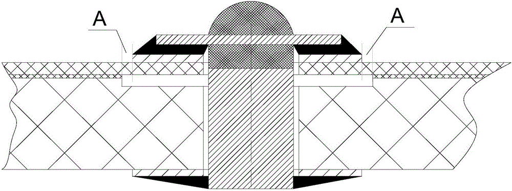
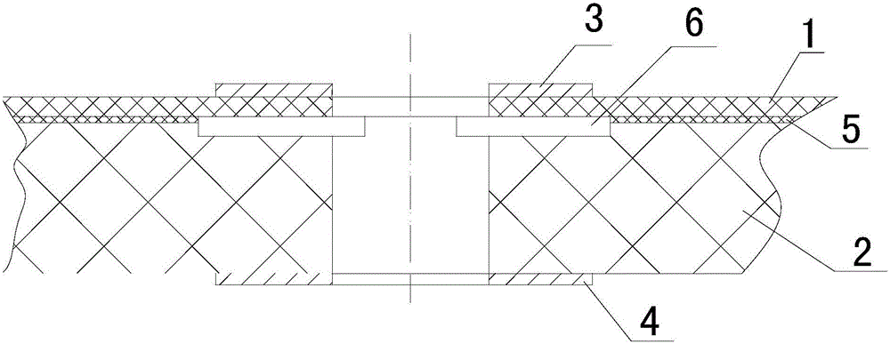
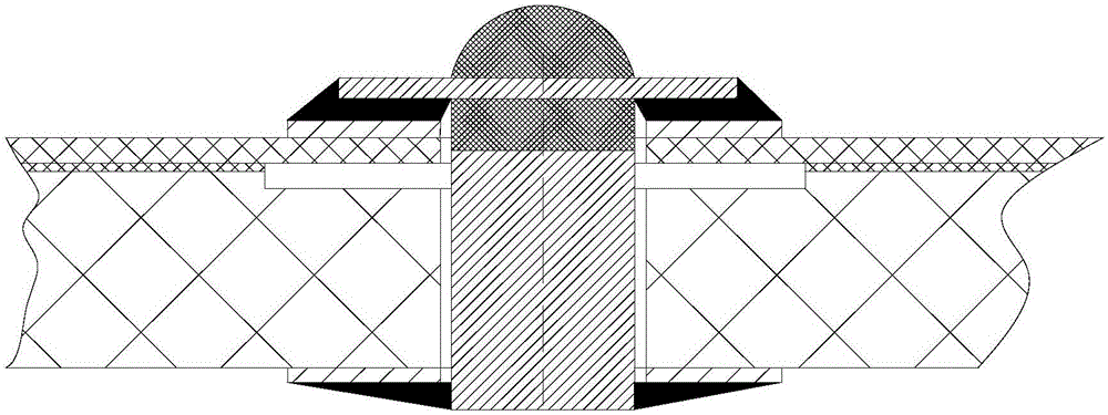
[0028] The flexible board 1 is designed to be made of polyimide material, with conductive patterns and two top-layer pads 3 laid on the upper surface. The top-layer pads 3 are rectangular in shape and 4×1.5mm in size. The rigid board 2 is an epoxy glass cloth board with conductive patterns and bottom pads 4 on its lower surface, and the adhesive 5 is made of prepreg; the upper surface of the rigid board 2 is designed with two grooves 6, the shape of the grooves is rectangular, and the size It is 4.5×2mm, and the groove depth is 0.2mm. The lower surface of the flexible board 1 and the upper surface of the rigid board 2 are bonded together by an adhesive 5 to form a complete printed circuit board. During the bonding process, ensure that each of the flexible board 1 and the rigid board 2 The corresponding position accuracy of the conductive pattern, the error is less than ±0.1mm.

[0029] The bonding material is a prepreg material commonly used in the PCB industry. The shape of ...

Embodiment 2

[0034] The flexible board 1 is designed to be made of polyimide material, with a conductive pattern and two top-layer pads 3 arranged on the upper surface. The top-layer pad 3 is square in shape and 2×2mm in size. The rigid board 2 is an epoxy glass cloth board with conductive patterns and bottom pads 4 on its lower surface, and the adhesive 5 is a prepreg; the upper surface of the rigid board 2 is designed with two grooves 6, the shape of the grooves is square, and the size It is 3×3mm, and the groove depth is 0.3mm. The lower surface of the flexible board 1 and the upper surface of the rigid board 2 are bonded together by an adhesive 5 to form a complete printed circuit board. During the bonding process, ensure that each of the flexible board 1 and the rigid board 2 The corresponding position accuracy of the conductive pattern, the error is less than ±0.1mm.

[0035] The bonding material is a prepreg material commonly used in the PCB industry. The shape of the bonding glue is...


PUM


Abstract

A printed circuit board structure for partially eliminating thermal mismatching in the thickness direction comprises a flexible board, a rigid board and a binder. A groove is formed in the upper surface of the rigid board. The lower surface of the flexible board and the upper surface of the rigid board are bound into a whole through adhesives. The groove forms a cavity. A through hole in the flexible board and a through hole in the rigid board are used for installing an element and are concentric and the same in size. Top layer welding plates are arranged on the upper surface of the flexible board and distributed around the through hole, for installing the element, of the flexible board. According to the printed circuit board structure, a traditional printed circuit board is innovated; for a through hole device which needs to be welded to the upper surface and the lower surface of the printed circuit board, an existing structure that a welding plate is arranged on the upper surface and the lower surface of the printed circuit board after a hole is directly punched in a rigid printed circuit board is designed into a printed circuit board structure integrating partial hollowness and rigidity; the problem that thermal mismatching exists between a traditional printed circuit board and the device in the thickness direction is thoroughly solved.

Description

technical field [0001] The invention relates to a printed circuit board structure for partially eliminating heat mismatch in the thickness direction, belonging to the field of printed circuit board design. Background technique [0002] Printed circuit boards are key components in electronic products, and certain electrical functions can be realized after electronic components are installed on them. The commonly used printed circuit board material is epoxy glass cloth board, and its thermal expansion coefficient in the thickness direction is about 65ppm / °C (when the temperature is less than 120°C). When this type of printed circuit board is used to install a through-hole optoelectronic device, since the device must form solder joints on the upper and lower surfaces of the printed circuit board, the thermal expansion coefficient of the metal body of the device is only 5-7ppm / °C , There is a serious thermal expansion coefficient mismatch between the device and the printed circ...

Claims


Application Information

Patent Timeline
Patent Type & Authority Patents(China)
IPC IPC(8): H05K1/02H05K1/03H05K1/11H05K1/18
Inventor 王修利李睿严贵生丁颖董芸松陆娇娣王友平崔赪旻刘磊
Owner BEIJING INST OF CONTROL ENG
Why Eureka
Try Eureka