Microfluidic chip based on optical detection and preparation method thereof

A microfluidic chip, optical detection technology, applied in the fields of biochemical analysis, medical diagnosis and bioengineering, can solve problems such as reducing device stability, increasing process complexity, deformation, etc., to improve detection accuracy, eliminate channel surface roughness, Simple preparation process

Active Publication Date: 2014-12-31
黄辉 +2
View PDF12 Cites 10 Cited by
  • Summary
  • Abstract
  • Description
  • Claims
  • Application Information

AI Technical Summary

Problems solved by technology

Among them, the FP resonant cavity sensor has the highest detection accuracy (up to 10 -8 Refractive index unit), the preparation process is relatively simple; however, in order to obtain good optical performance, the surface of the sample channel in the sensor is required to be flat and smooth; therefore, an additional corrosion stop layer needs to be introduced to avoid surface damage caused by the corrosion of the channel Rough, which increases process complexity
In addition, sensors are usually composed of different materials, and the thermal expansion coefficients of different materials are different (referred to as "thermal mismatch"), so temperature changes will cause changes in thermal stress in the sensor, resulting in deformation and lower device performance. stability

Method used


Image

  • Microfluidic chip based on optical detection and preparation method thereof
  • Microfluidic chip based on optical detection and preparation method thereof
  • Microfluidic chip based on optical detection and preparation method thereof

Examples


Embodiment 1

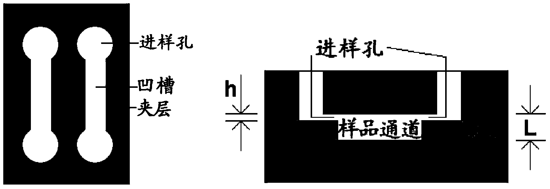
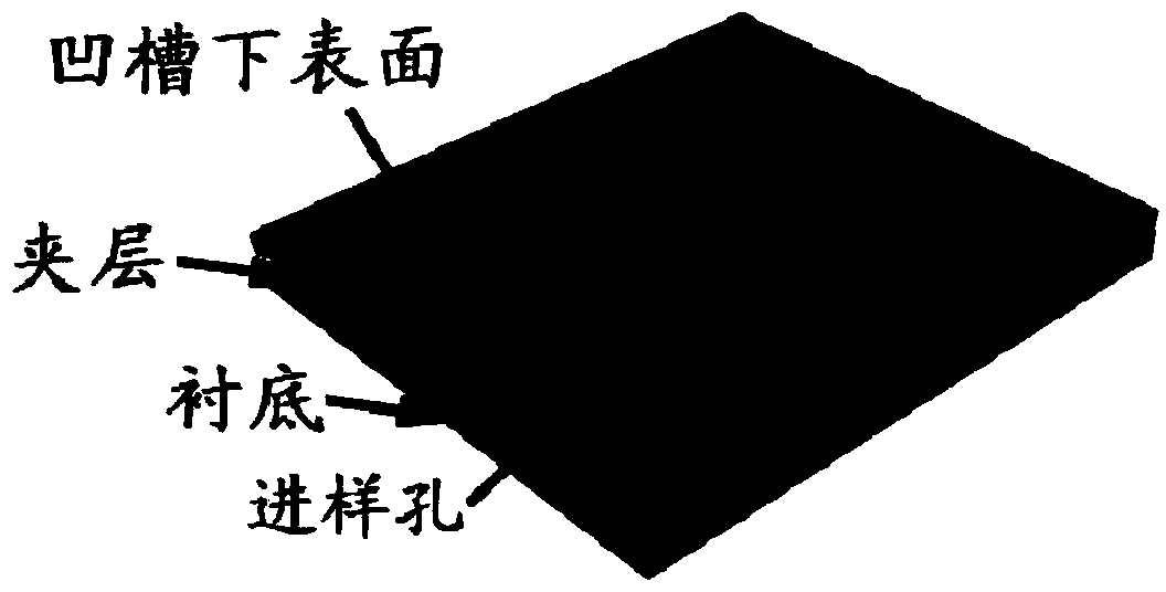
[0030] refer to Figure 1 to Figure 4 , the present invention provides a microfluidic chip based on optical detection, including an upper substrate layer, a lower substrate layer, and an interlayer all made of glass, the interlayer is located in the middle of the two substrate layers, and the interlayer is provided with a sample channel And the sampling hole, the sample channel is composed of the groove structure penetrated in the interlayer and the substrate surface; the corrosion depth of the interlayer sampling hole in this embodiment is equal to the thickness of the interlayer.

[0031] The present invention also provides a method for preparing a microfluidic chip based on optical detection, which mainly includes the following steps:

[0032] In the first step, utilize an etching process to prepare groove structures and injection holes on the glass interlayer. The etching process in this embodiment is chemical etching, wherein the grooves penetrate the glass interlayer (su...

Embodiment 2

[0035] refer to Figure 1 to Figure 4 , the present invention provides a microfluidic chip based on optical detection, comprising an interlayer made of glass, an upper substrate layer and a lower substrate layer made of silicon, the interlayer is located in the middle of the two substrate layers, and the interlayer is set There are sample channel and sampling hole, and described sample channel is made of the groove structure that penetrates in the interlayer and the substrate surface; The corrosion depth of the interlayer sampling hole described in the present embodiment is equal to 0.9 times of the thickness of the interlayer; The substrate is provided with a sampling hole, and the substrate sampling hole is connected to the interlayer sampling hole;

[0036] The present invention also provides a method for preparing a microfluidic chip based on optical detection, which mainly includes the following steps:

[0037] In the first step, the groove structure and the sampling hol...

Embodiment 3

[0040] refer to Figure 1 to Figure 4 , the present invention provides a microfluidic chip based on optical detection, comprising an interlayer made of silicon, an upper substrate layer and a lower substrate layer made of glass, the interlayer is located in the middle of the two substrate layers, and the interlayer is set There are sample channel and sampling hole, and described sample channel is made of the groove structure that penetrates in the interlayer and the substrate surface; The corrosion depth of the interlayer sampling hole described in the present embodiment is equal to 0.5 times of the thickness of interlayer; The substrate is provided with a sampling hole, and the substrate sampling hole is connected to the interlayer sampling hole; the glass substrate is coated with Si / SiO 2 film.

[0041] The present invention also provides a method for preparing a microfluidic chip based on optical detection, which mainly includes the following steps:

[0042] The first ste...


PUM


Abstract

The invention relates to a microfluidic chip based on optical detection and a preparation method thereof. A microfluidic chip based on optical detection includes an upper substrate layer, a lower substrate layer and an interlayer. The interlayer is positioned between the two substrate layers, the interlayer is provided with a sample channel and an injection hole, and the sample channel comprises a groove structure penetrating through the interlayer and substrate surfaces. The preparation method comprises the following steps: 1, preparing the groove structure and the injection hole in the interlayer, wherein the groove structure penetrates through the interlayer; and 2, bonding the interlayer with groove structure and the two substrates together, so that side wall of the groove and the substrate surfaces constitute the sample passage. The invention has the beneficial effects that the surface of the microfluidic chip sample channel is smooth, so no thermal mismatch exists; and arrangement of the injection hole leads to turbulence within the sample channel, so as to improve the detection accuracy. Therefore, the invention has the characteristics of simple preparation process, high stability and high detection sensitivity.

Description

technical field [0001] The invention relates to a microfluidic chip for detecting gas or liquid samples and a sensor comprising the microfluidic chip, in particular to a microfluidic chip based on optical detection and a preparation method thereof, which can be applied to biochemical analysis , medical diagnosis and bioengineering. Background technique [0002] The integration of optical detection technology and microfluidic chip technology has given birth to "optofluidic" sensors (Nature Photon., 5(10), 591-597(2011)). The use of optofluidic sensors to analyze and detect gas or liquid samples has the advantages of label-free, real-time dynamics, and demand for trace samples. [0003] At present, there are three main types of optofluidic sensors: microring resonator sensors (Appl. Phys. Lett., 97, 011105 (2010)); surface plasmon resonance sensors (Anal. (2010)); and Fabry-Pérot (FP) resonant cavity sensors (Appl. Phys. Lett., 102, 163701 (2013)). Among them, the FP resona...

Claims


Application Information

Patent Timeline
Patent Type & Authority Applications(China)
IPC IPC(8): G01N35/00G01N21/01
Inventor 黄辉渠波刘蓬勃
Owner 黄辉
Why Eureka
Try Eureka