Superlattice mid- and long-wave dual-band infrared detector chip and preparation method thereof

An infrared detector, dual-band technology, used in semiconductor devices, final product manufacturing, sustainable manufacturing/processing, etc., can solve the problems of not achieving passivation, discontinuity, and lack of uniform coverage, and achieve better use effects. Reduces dark current, eliminates thermal mismatch effects

Active Publication Date: 2022-07-05
SUZHOU KUNYUAN OPTOELECTRONICS CO LTD
View PDF0 Cites 0 Cited by
  • Summary
  • Abstract
  • Description
  • Claims
  • Application Information

AI Technical Summary

Problems solved by technology

[0006] Since the long-wave detector chip in the superlattice adopts a laminated structure with upper and lower bands, the thickness of the working layer (table thickness) is much larger than that of some single-band chips. The aspect ratio b / a of these inter-mesa trenches will be found when the infrared detector chip in the superlattice is passivated for long-wave (medium-wave 3-5 microns, long-wave 8-14 microns) (see image 3 As shown) is more than 2 times, the passivation layer deposited on the side wall often has a discontinuous phenomenon, so that the middle section of the side of the high mesa is not evenly covered (see image 3 shown), similar to the fact that there is no snow on the side of the deep gutter after falling snow, so the passivation effect is not achieved

Method used


Image

  • Superlattice mid- and long-wave dual-band infrared detector chip and preparation method thereof
  • Superlattice mid- and long-wave dual-band infrared detector chip and preparation method thereof
  • Superlattice mid- and long-wave dual-band infrared detector chip and preparation method thereof

Examples


Embodiment Construction

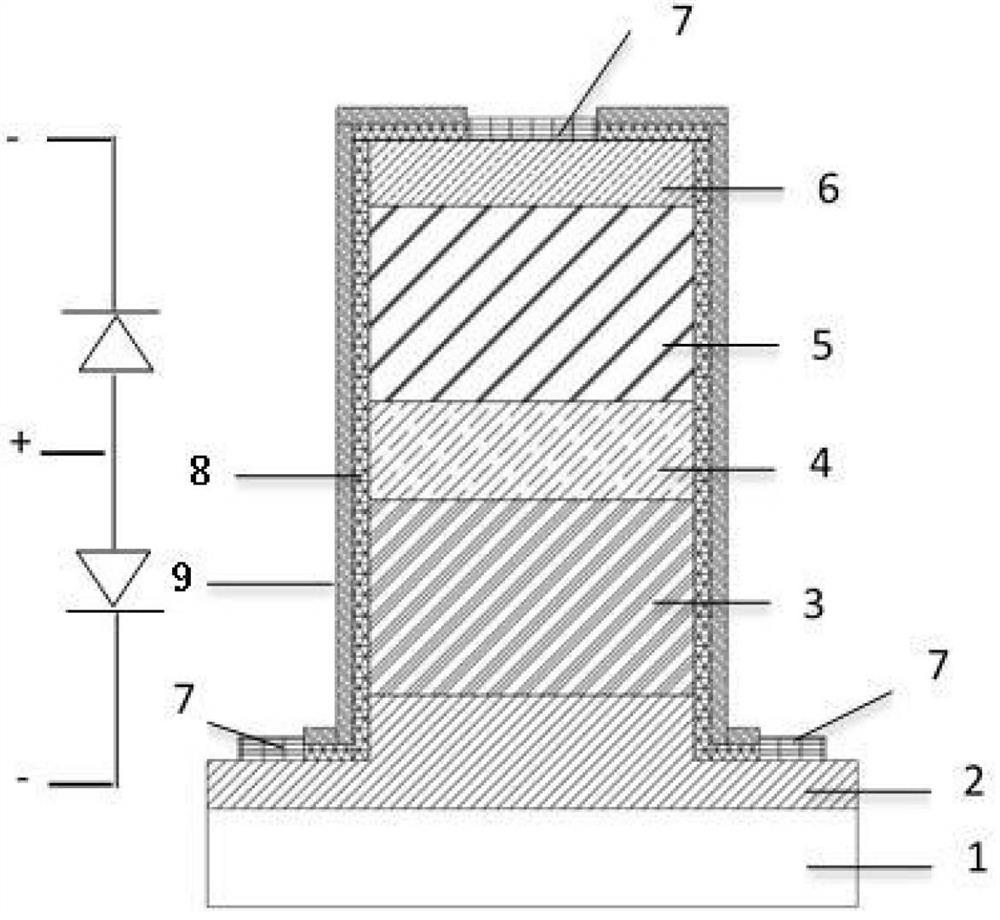
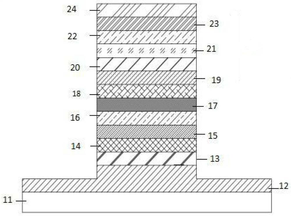
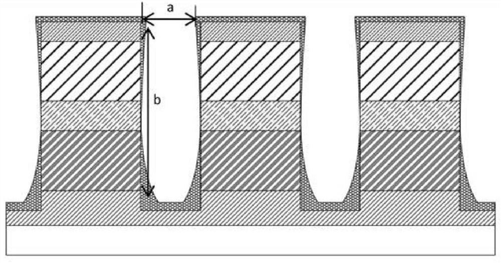
[0049] The technical solutions in the embodiments of the present invention will be clearly and completely described below with reference to the accompanying drawings in the embodiments of the present invention. Obviously, the described embodiments are only a part of the embodiments of the present invention, rather than all the embodiments. The components of the embodiments of the invention generally described and illustrated in the drawings herein may be arranged and designed in a variety of different configurations. Thus, the following detailed description of the embodiments of the invention provided in the accompanying drawings are not intended to limit the scope of the invention as claimed, but are merely representative of selected embodiments of the invention. Based on the embodiments of the present invention, those skilled in the art should understand that: they can still modify the technical solutions of the embodiments, or perform equivalent replacements on some of the t...


PUM

PropertyMeasurementUnit
thicknessaaaaaaaaaa
thicknessaaaaaaaaaa

Abstract

The invention discloses a method for preparing a superlattice medium and long-wave dual-band infrared detector chip, which includes providing a substrate, growing a dual-band antimonide superlattice material on the substrate, The composite passivation process is carried out on the high table surface. During passivation, it includes providing an anode vulcanization electrolyte. The anode vulcanization electrolyte includes a mixed solution of anhydrous sodium sulfide and dimethyl sulfoxide. The anode vulcanization treatment is carried out by using the anode vulcanization electrolyte. The sulfide film is grown on the high mesa of the band stack, the sulfide film covers the high mesa, and extends down from the high mesa to the sidewall of the high mesa; Al is deposited on the sulfide film 2 O 3 The film forms a composite passivation film. The present invention grows sulfide thin films and Al 2 O 3 The film forms a composite passivation film, which reduces the dark current of the device while solving the interface state problem, significantly improves the quantum efficiency and detection rate of the detector, and achieves a good passivation effect.

Description

technical field [0001] The invention relates to the technical field of manufacture of superlattice infrared detectors, in particular to an antimonide superlattice medium and long-wave dual-band infrared detector chip and a preparation method thereof. Background technique [0002] The development of a new generation of infrared detectors requires enhanced capabilities such as multi-band capabilities, large-scale pixels, and higher frame rates and better thermal resolution. The current leading candidates for detectors are HgCdTe (MCT), quantum well infrared photodetectors (QWIPs) and, more recently, class II strained layer superlattices (T2SL). Compared with HgCdTe, antimonide-based T2SL detectors have several advantages, such as the availability of large-area lattice-matched substrates, and are based on a more mature III-V process technology. However, the quantum efficiency of QWIPs is very low, while in T2SL, the detector parameters such as quantum efficiency, responsivity ...

Claims


Application Information

Patent Timeline
Patent Type & Authority Patents(China)
IPC IPC(8): H01L31/18H01L31/0216H01L31/0304H01L31/036H01L31/101
CPCY02P70/50
Inventor 陈意桥孙维国颜全
Owner SUZHOU KUNYUAN OPTOELECTRONICS CO LTD
Why Eureka
Try Eureka