Superlattice medium-long wave dual-band infrared detector chip and preparation method thereof

An infrared detector and dual-band technology, applied in semiconductor devices, final product manufacturing, sustainable manufacturing/processing, etc., can solve the problems of no uniform coverage, no passivation, discontinuity, etc., to eliminate thermal mismatch, The effect of using is better and the effect of reducing dark current

Active Publication Date: 2022-04-08
苏州焜原光电有限公司
View PDF4 Cites 0 Cited by
  • Summary
  • Abstract
  • Description
  • Claims
  • Application Information

AI Technical Summary

Problems solved by technology

[0006] Since the long-wave detector chip in the superlattice adopts a laminated structure with upper and lower bands, the thickness of the working layer (table thickness) is much larger than that of some single-band chips. The aspect ratio b / a of these inter-mesa trenches will be found when the infrared detector chip in the superlattice is passivated for long-wave (medium-wave 3-5 microns, long-wave 8-14 microns) (see image 3 As shown) is more than 2 times, the passivation layer deposited on the side wall often has a discontinuous phenomenon, so that the middle section of the side of the high mesa is not evenly covered (see image 3 shown), similar to the fact that there is no snow on the side of the deep gutter after falling snow, so the passivation effect is not achieved

Method used


Image

  • Superlattice medium-long wave dual-band infrared detector chip and preparation method thereof
  • Superlattice medium-long wave dual-band infrared detector chip and preparation method thereof
  • Superlattice medium-long wave dual-band infrared detector chip and preparation method thereof

Examples


Embodiment Construction

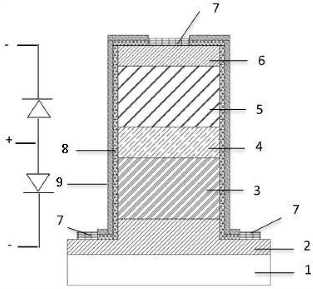
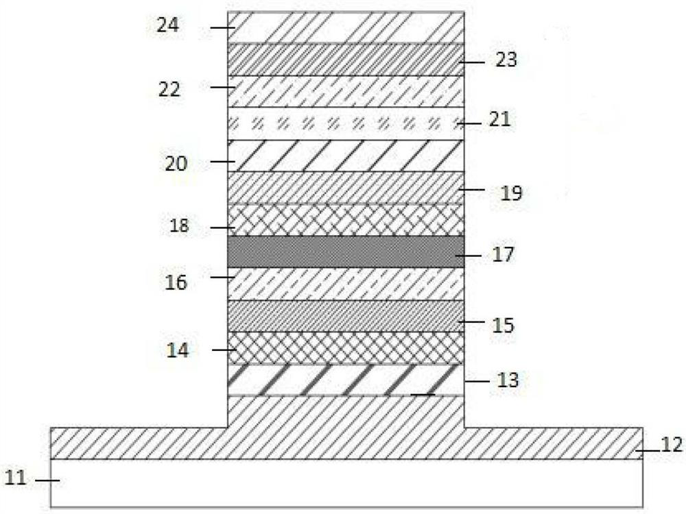
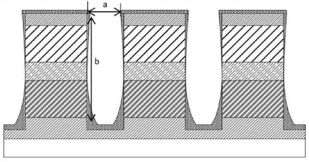
[0049] The following will clearly and completely describe the technical solutions in the embodiments of the present invention with reference to the accompanying drawings in the embodiments of the present invention. Obviously, the described embodiments are only some, not all, embodiments of the present invention. The components of the embodiments of the invention generally described and illustrated in the figures herein may be arranged and designed in a variety of different configurations. Accordingly, the following detailed description of the embodiments of the invention provided in the accompanying drawings is not intended to limit the scope of the claimed invention, but merely represents selected embodiments of the invention. Based on the embodiments of the present invention, those skilled in the art should understand that it is still possible to modify the technical solutions of each embodiment, or perform equivalent replacements for some of the technical features; and these...


PUM

PropertyMeasurementUnit
Thicknessaaaaaaaaaa

Abstract

The invention discloses a superlattice medium-long wave dual-band infrared detector chip preparation method, which comprises the following steps: providing a substrate, growing a dual-band laminated antimonide superlattice material on the substrate, and carrying out a composite passivation process on a high table top of a dual-band laminated detector chip, the anode vulcanization electrolyte comprises mixed anhydrous sodium sulfide and a dimethyl sulfoxide solution; performing anode vulcanization treatment by using an anode vulcanization electrolyte, growing a sulfide film on the dual-band laminated high mesa, and enabling the sulfide film to cover the high mesa and extend downwards from the upper edge of the high mesa to the side wall of the high mesa; and depositing an Al2O3 thin film on the sulfide thin film to form a composite passivation thin film. The sulfide thin film and the Al2O3 thin film are grown to form the composite passivation thin film, so that the interface state problem is solved, the dark current of the device is reduced, the quantum efficiency and the detection rate of the detector are remarkably improved, and a good passivation effect is achieved.

Description

technical field [0001] The invention relates to the technical field of superlattice infrared detector manufacturing, in particular to a long-wave dual-band infrared detector chip in an antimonide superlattice and a preparation method thereof. Background technique [0002] The development of next-generation infrared detectors requires enhanced capabilities such as multi-band capabilities, large-scale pixels, and higher frame rates and better thermal resolution. The main candidates for current detectors are HgCdTe (MCT), quantum well infrared photodetectors (QWIP) and more recently type II strained layer superlattices (T2SL). Antimonide-based T2SL detectors have several advantages over HgCdTe, such as the availability of large-area lattice-matched substrates and are based on a more mature III-V process technology. However, the quantum efficiency of QWIPs is very low, while in T2SL, the detector parameters such as quantum efficiency, responsivity, and detection rate are compar...

Claims


Application Information

Patent Timeline
IPC IPC(8): H01L31/18H01L31/0216H01L31/0304H01L31/036H01L31/101
CPCY02P70/50
Inventor 陈意桥孙维国颜全
Owner 苏州焜原光电有限公司
Why Eureka
Try Eureka