Silicon pressure chip structure design and process

A pressure and chip technology, applied in the multi-layer silicon structure pressure chip and process field, to achieve the effect of improving stability, improving stability and consistency, and eliminating excessive high temperature leakage current

Active Publication Date: 2016-08-31
慧石(上海)测控科技有限公司
View PDF6 Cites 0 Cited by
  • Summary
  • Abstract
  • Description
  • Claims
  • Application Information

AI Technical Summary

Problems solved by technology

Under high temperature conditions, especially when the temperature is greater than 200 degrees, the current glue cannot fully meet these requirements

Method used


Image

  • Silicon pressure chip structure design and process
  • Silicon pressure chip structure design and process
  • Silicon pressure chip structure design and process

Examples


Embodiment Construction

[0030] In order to make the technical means, creative features, goals and effects achieved by the present invention easy to understand, the present invention will be further described below in conjunction with specific embodiments.

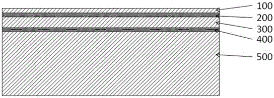
[0031] Such as figure 1 As shown, the present invention adopts a multilayer (three-layer) silicon structure, which includes a first layer of single crystal silicon 100, a first layer of insulating layer 200, a second layer of single crystal silicon 300, and a second layer of single crystal silicon 300 arranged in sequence from top to bottom. The second layer of insulating layer 400 and the third layer of single crystal silicon 500. The thickness, resistivity, and other physical and chemical properties of each layer can be determined according to the performance requirements of the strain gauge when manufacturing the multi-layer (three-layer) silicon structure.

[0032] In this implementation, the first layer of single crystal silicon 100 is (100)...


PUM

PropertyMeasurementUnit
thicknessaaaaaaaaaa
thicknessaaaaaaaaaa
thicknessaaaaaaaaaa

Abstract

The invention discloses a structural design and process for manufacturing a pressure chip by the adoption of a multilayer silicon structure. The process includes the steps that (1) a silicon-insulating layer-silicon-insulating layer-silicon multilayer (three-layer) silicon structure is adopted for manufacturing of the pressure chip, a full-bridge piezoresistance element, a connecting point and a silicon sealing strip are arranged on first-layer silicon, grooves are formed around the piezoresistance element and the connecting point, and a cavity with an island-type structure is formed in third-layer silicon of the multilayer (three-layer) silicon structure; (2) another conventional SOI piece is selected as a sealing structure, and a silicon sealing strip and a silicon connecting column are arranged on first-layer silicon of the SOI piece; (3) a silicon-silicon bonding technology is adopted, and the multilayer (three-layer) silicon structure and the conventional SOI piece are bonded to form a multilayer (five-layer) silicon structure; (4) second-layer silicon of the conventional SOI piece is thinned, and a through hole is formed in the second-layer silicon of the conventional SOI piece by means of plasma dry etching; (5) insulating layers are deposited on the surface of the second-layer silicon of the conventional SOI piece and the inner wall of the through hole, conducting materials are deposited at the through hole, and accordingly electrical connecting points are formed.

Description

technical field [0001] The invention relates to the field of pressure sensors, in particular to a pressure chip with a multi-layer silicon structure and a process. Background technique [0002] Micro-electro-mechanical technology, also known as MEMS (Micro-Electro-Mechanical-System) technology, is a high-tech technology that miniaturizes mechanical and electronic devices, and is especially suitable for large-scale manufacturing of high-performance micro-mechanical and electronic devices, such as miniature pressure sensors. Micro accelerometer, micro gyroscope, etc. Combining integrated circuits and mechanical structures, these microelectromechanical devices feature powerful functions, high precision, and high reliability. [0003] The MEMS pressure sensor relies on a layer of pressure film to sense the pressure of the external medium. When the piezoresistive element on the pressure film receives the pressure transmitted from the pressure film, its electrical properties chan...

Claims


Application Information

Patent Timeline
Patent Type & Authority Patents(China)
IPC IPC(8): G01L9/06G01L1/18B81B7/00B81C1/00
Inventor 张鹏吴宽洪张涛熊建功
Owner 慧石(上海)测控科技有限公司
Why Eureka
Try Eureka