Cleaning system and method

A cleaning system and cleaning technology, applied in the field of cleaning systems, can solve problems such as poor substrates and dust falling, and achieve the effect of improving yield and reducing defective substrates

Active Publication Date: 2014-08-06
BEIJING BOE OPTOELECTRONCIS TECH CO LTD
View PDF5 Cites 12 Cited by
  • Summary
  • Abstract
  • Description
  • Claims
  • Application Information

AI Technical Summary

Problems solved by technology

[0003] In practical applications, when the motherboard is moved to the exposure lamp, dust usually falls on the motherboard, resulting in a pattern of dust on the substrate after exposure, resulting in defective substrates.

Method used


Image

  • Cleaning system and method
  • Cleaning system and method
  • Cleaning system and method

Examples


Embodiment Construction

[0040] The technical solutions of the present invention will be further elaborated below in conjunction with the accompanying drawings and specific embodiments.

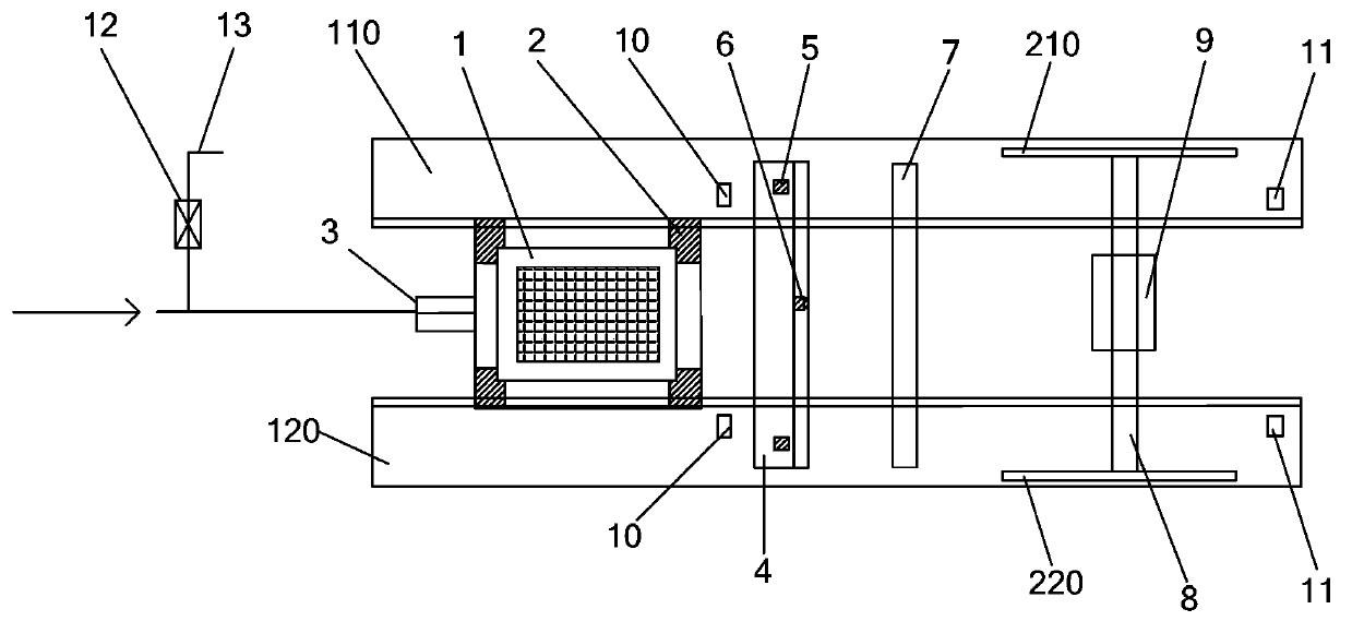
[0041] A structural schematic diagram of a cleaning system provided by an embodiment of the present invention, as figure 1 As shown, the motherboard 1 is placed on the motherboard frame 2, which can ensure that the position of the motherboard 1 is accurate, and the motherboard frame 2 can move at a constant speed along the first track modules 110 and 120 under the action of the cylinder 3. A group of track modules, the first track modules 110 and 110 provide moving tracks and supports for the motherboard frame 2; the electromagnetic control valve 12 controls the on-off of the gas, when the electromagnetic control valve 12 is opened, it is negative pressure gas input to control the motherboard frame 2 Move in one direction along the first track modules 110 and 120; when the solenoid control valve 12 is closed, positiv...


PUM


Abstract

The invention discloses a cleaning system and method. The system comprises a first cleaning device, an optical detecting device and a second cleaning device, wherein the first cleaning device is used for cleaning a mother board in a gas cleaning manner; the optical detecting device is used for performing optical detection on the gas-cleaned mother board, and judging whether dust exists on the mother board or not and determining position coordinates of the dust; the second cleaning device is used for cleaning the dust on the corresponding position coordinates on the mother board according to the dust position coordinates determined by the optical detecting device. With adoption of the cleaning system and method, dust on the mother board can be effectively removed; the frequency of an unhealthy phenomenon occurring to the substrate can be reduced; the product yield can be improved.

Description

technical field [0001] The invention relates to dust cleaning technology, in particular to a cleaning system and method. Background technique [0002] In the field of liquid crystal display panel or flat panel manufacturing, the pattern on the master board is usually irradiated on the substrate coated with uniform photosensitive material by means of instant exposure of the pre-engraved master board under the exposure lamp, so that the light irradiated The properties of the photosensitive material change, and then the photosensitive material irradiated by light is washed away by chemicals, and finally the photosensitive material pattern is obtained on the substrate. [0003] In practical applications, when the motherboard is moved to the exposure lamp, dust usually falls on the motherboard, resulting in a pattern of the dust on the substrate after exposure, resulting in defective substrates. Contents of the invention [0004] In view of this, the main purpose of the presen...

Claims


Application Information

Patent Timeline
Patent Type & Authority Applications(China)
IPC IPC(8): B08B7/04B08B5/00B08B1/04
CPCB08B1/04B08B5/02B08B5/04B08B7/04
Inventor 焦宇王晏酩刘杰
Owner BEIJING BOE OPTOELECTRONCIS TECH CO LTD
Why Eureka
Try Eureka