Touch screen and display device

A touch screen, consistent technology, applied in optics, instrumentation, electrical digital data processing, etc., can solve the problems of touch screen border expansion, signal disorder, large touch blind area, etc., to ensure touch performance, achieve accuracy, and avoid misjudgment Effect

Active Publication Date: 2014-08-06
BOE TECH GRP CO LTD +1
View PDF6 Cites 62 Cited by
  • Summary
  • Abstract
  • Description
  • Claims
  • Application Information

AI Technical Summary

Problems solved by technology

In order to simplify the number of layers in the design, the wires in the lead-out line and the self-capacitance electrodes are generally arranged on the same layer. More wires will cause a large touch blind area. The touch blind area refers to the concentration of wires in the touch screen. In this area, the signal in this touch blind area is relatively disordered, so it is called a touch blind area, that is, the touch performance in this area cannot be guaranteed.
figure 1 30 self-capacitance electrodes are used as an example for illustration. 30 self-capacitance electrodes need 30 wires to lead them to the frame. A total of 10 wires are needed in the place where the wires are densest, which will cause a large touch blind area.
[0006] In addition, due to the large number of wires, there will also be too many peripheral wires arranged at the frame and connected to the wires one by one, which will cause the frame of the touch screen to expand, which is not conducive to the narrow frame design.

Method used


Image

  • Touch screen and display device
  • Touch screen and display device
  • Touch screen and display device

Examples


Embodiment Construction

[0045] The specific implementation manners of the touch screen and the display device provided by the embodiments of the present invention will be described in detail below with reference to the accompanying drawings.

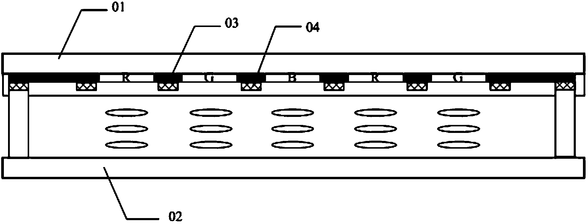
[0046] The thickness and shape of each film layer in the drawings do not reflect the real scale, and the purpose is only to illustrate the content of the present invention.

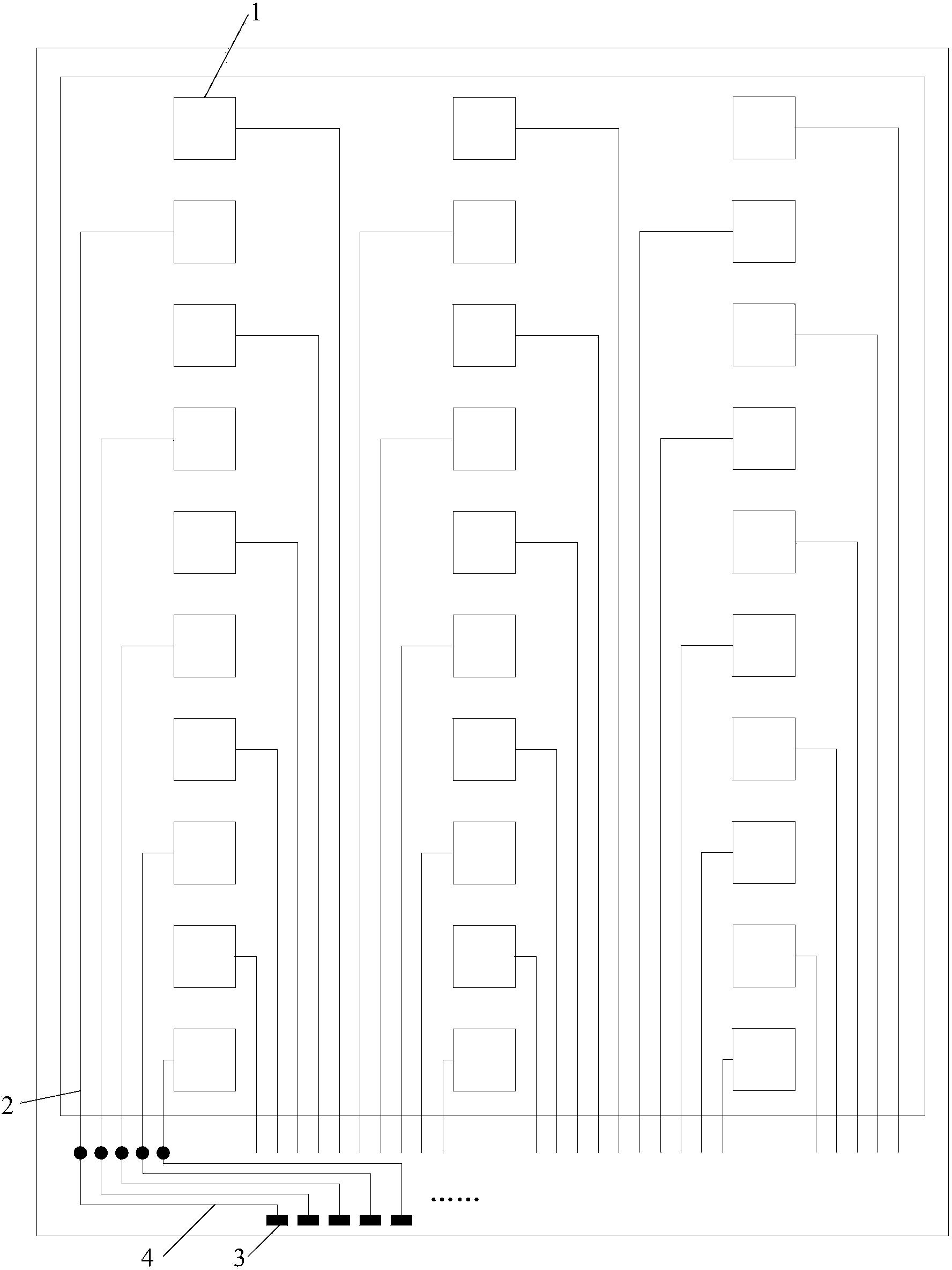
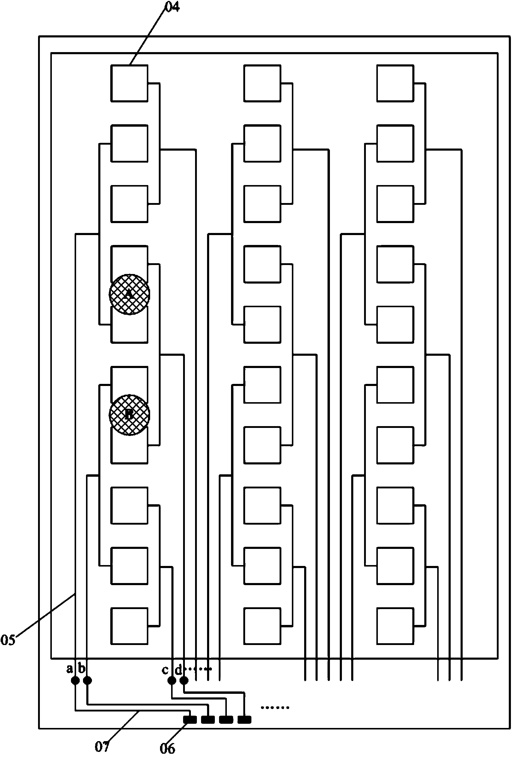
[0047] A touch screen provided by an embodiment of the present invention, such as image 3 shown, including:

[0048] A plurality of self-capacitance electrodes 04 arranged on the same layer and independent of each other;

[0049] Such as image 3 As shown, the self-capacitance electrode 04 is connected to a plurality of wires 05 at the frame of the touch screen; wherein, each wire 05 is electrically connected to at least two self-capacitance electrodes 04 arranged at intervals, and is electrically connected to each wire 05. The connected capacitor electrodes 04 do not overlap with each...


PUM


Abstract

The invention discloses a touch screen and a display device. A plurality of self-capacitance electrodes are arranged on the same layer and independent to each other by means of the self-capacitance principle. Two or more self-capacitance electrodes arranged alternatively are connected with a frame of the touch screen through a lead and then connected with a touch detection chip through a corresponding periphery wire to perform touch position detection. When the human body touches the screen, the touch detection chip determines the touch position by judging changes of capacitance of the adjacent self-capacitance electrodes connected with different leads, and accuracy of touch sensing is achieved. By means of the mode that a plurality of self-capacitance electrodes which are not adjacent to each other are connected with one lead correspondingly, total quantity of the leads in the touch screen can be reduced effectively, the area of the touch blind region is decreased, and touch performance is ensured. In addition, due to decrease of the quantity of the leads, the quantity of the periphery wires corresponding to the leads is decreased, and design of the narrow frame of the touch screen is facilitated.

Description

technical field [0001] The present invention relates to the field of touch technology, in particular to a touch screen and a display device. Background technique [0002] With the rapid development of display technology, touch screen panels (Touch Screen Panels) have gradually spread throughout people's lives. At present, touch screens can be divided into three types according to their structure: Add on Mode Touch Panel, On Cell Touch Panel, and InCell Touch Panel. Among them, the plug-in touch screen is produced separately from the touch screen and Liquid Crystal Display (LCD), and then bonded together to form a touch-enabled LCD screen. The plug-in touch screen has high production costs and low light transmittance. , The module is thicker and other shortcomings. In the touch screen, the touch electrodes of the touch screen are embedded in the liquid crystal display, which can reduce the overall thickness of the module and greatly reduce the production cost of the touch s...

Claims


Application Information

Patent Timeline
Patent Type & Authority Applications(China)
IPC IPC(8): G06F3/044G02F1/1333
CPCG06F3/0412G06F3/04164G06F3/04166G06F3/0443G06F2203/04103G06F2203/04112
Inventor 丁小梁王海生刘英明任涛
Owner BOE TECH GRP CO LTD
Why Eureka
Try Eureka