Peeling device and peeling method of substrate, and manufacturing method of electronic device

A technology for peeling off devices and substrates, which is applied in the fields of semiconductor/solid-state device manufacturing, electrical components, circuits, etc.

Active Publication Date: 2014-08-06
ASAHI GLASS CO LTD
View PDF4 Cites 16 Cited by
  • Summary
  • Abstract
  • Description
  • Claims
  • Application Information

AI Technical Summary

Problems solved by technology

However, when the strength of the substrate decreases due to thinning, the handleability of the substrate deteriorates, so functional layers for electronic devices such as thin film transistors (TFT: ThinFilm Transistor) and color filters (CF: colorfilter) are formed on the surface of the substrate become difficult

Method used


Image

  • Peeling device and peeling method of substrate, and manufacturing method of electronic device
  • Peeling device and peeling method of substrate, and manufacturing method of electronic device
  • Peeling device and peeling method of substrate, and manufacturing method of electronic device

Examples


Embodiment Construction

[0044] Hereinafter, embodiments of a substrate peeling device, a peeling method, and an electronic device manufacturing method according to the present invention will be described with reference to the drawings.

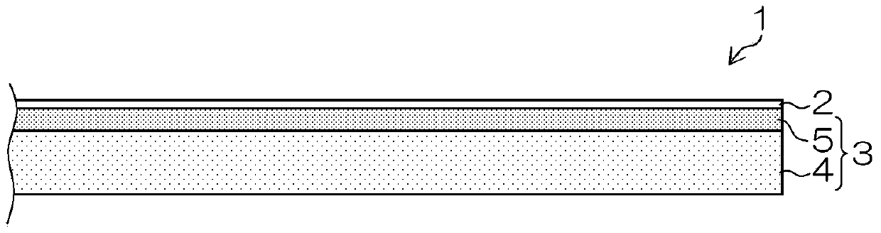
[0045] figure 1 It is an enlarged side view of main parts of the laminated board 1 used in the manufacturing process of an electronic device.

[0046] (Manufacturing method of electronic device)

[0047] In order to cope with the thinning of the substrate 2 used in electronic devices, the manufacturing method of the electronic device according to the embodiment has the following steps: constructing the laminated board 1 in which the front surface of the reinforcing plate 3 is pasted on the back surface of the substrate 2, and forming a laminated board 1 on the laminated board 1 A functional layer forming step of forming a functional layer on the surface of the substrate 2 ; and a peeling step of peeling between the substrate 2 on which the functional layer is forme...


PUM

PropertyMeasurementUnit
thicknessaaaaaaaaaa
thicknessaaaaaaaaaa

Abstract

The invention relates to a peeling device and peeling method of a substrate, and a manufacturing method of an electronic device. The peeling device of the substrate enables at least one of the substrate and a reinforcing plate for reinforcing the substrate to form flexural deflection and peels successively from an interface between the substrate and the reinforcing plate along a forward direction from one end side to the other end side. The peeling device of the substrate comprises a peeling component for pressing the substrate and the reinforcing plate with the interface peeled toward an opposite close direction.

Description

technical field [0001] The present invention relates to a peeling device and a peeling method for peeling between a substrate and a reinforcing plate, and a manufacturing method of an electronic device. Background technique [0002] In recent years, along with the reduction in thickness and weight of electronic devices such as display panels, solar cells, and thin-film secondary batteries, there has been a demand for thinner substrates used in electronic devices. However, when the strength of the substrate decreases due to thinning, the handleability of the substrate deteriorates, so functional layers for electronic devices such as thin film transistors (TFT: ThinFilm Transistor) and color filters (CF: colorfilter) are formed on the surface of the substrate become difficult. [0003] Therefore, a method has been proposed in which a laminate (in a broad sense, a laminate) is formed by detachably pasting the surface of a reinforcing plate on the back surface of the substrate,...

Claims


Application Information

Patent Timeline
Patent Type & Authority Applications(China)
IPC IPC(8): H01L21/683
CPCB65H3/08B65H3/16B65H41/00B65H29/56B65H2301/51122B65H2701/1752
Inventor 伊藤泰则宇津木洋泷内圭
Owner ASAHI GLASS CO LTD
Why Eureka
Try Eureka