Solid-state imaging element, method for driving same, and camera system

A technology of solid-state imaging device and pixel unit, which is applied in the direction of electrical components, electrical solid-state devices, and components of TV systems, etc., which can solve the problem of low resolution of the viewfinder and achieve the effect of suppressing whitening

Inactive Publication Date: 2014-08-06
SONY CORP
View PDF3 Cites 4 Cited by
  • Summary
  • Abstract
  • Description
  • Claims
  • Application Information

AI Technical Summary

Problems solved by technology

[0004] Also, such electronic devices often have a viewfinder for confirming the picture, but the resolution of the viewfinder is usually lower than that of the imaged image

Method used


Image

  • Solid-state imaging element, method for driving same, and camera system
  • Solid-state imaging element, method for driving same, and camera system
  • Solid-state imaging element, method for driving same, and camera system

Examples


no. 3 example

[0054] 3. Third Embodiment (Third Configuration Example of Solid-State Imaging Device)

[0055] 4. Fourth Embodiment (Configuration Example of Camera System)

no. 1 example

[0057] Figure 4 is a block diagram showing a configuration example of a solid-state imaging device (CMOS image sensor) mounted with a column-parallel ADC according to the first embodiment.

[0058] [Overall Configuration Example of Solid-State Imaging Device]

[0059] Such as Figure 4 As shown in , the solid-state imaging device 100 has a pixel unit 110 as an imaging portion, a vertical scanning circuit (row scanning circuit) 120 , a horizontal transfer scanning circuit (column scanning circuit) 130 , and a timing control circuit 140 .

[0060] Also, the solid-state imaging device 100 has pixel current sources 150D and 150U as column circuits, column parallel processing units 160D and 160U forming an ADC group, a digital-to-analog converter (DAC) 170, and an internal voltage generation circuit (bias circuit) 180 .

[0061] In this embodiment, the pixel signal readout unit is formed by a horizontal transfer scanning circuit 130 , a pixel current source 150 , a column paral...

no. 1 example

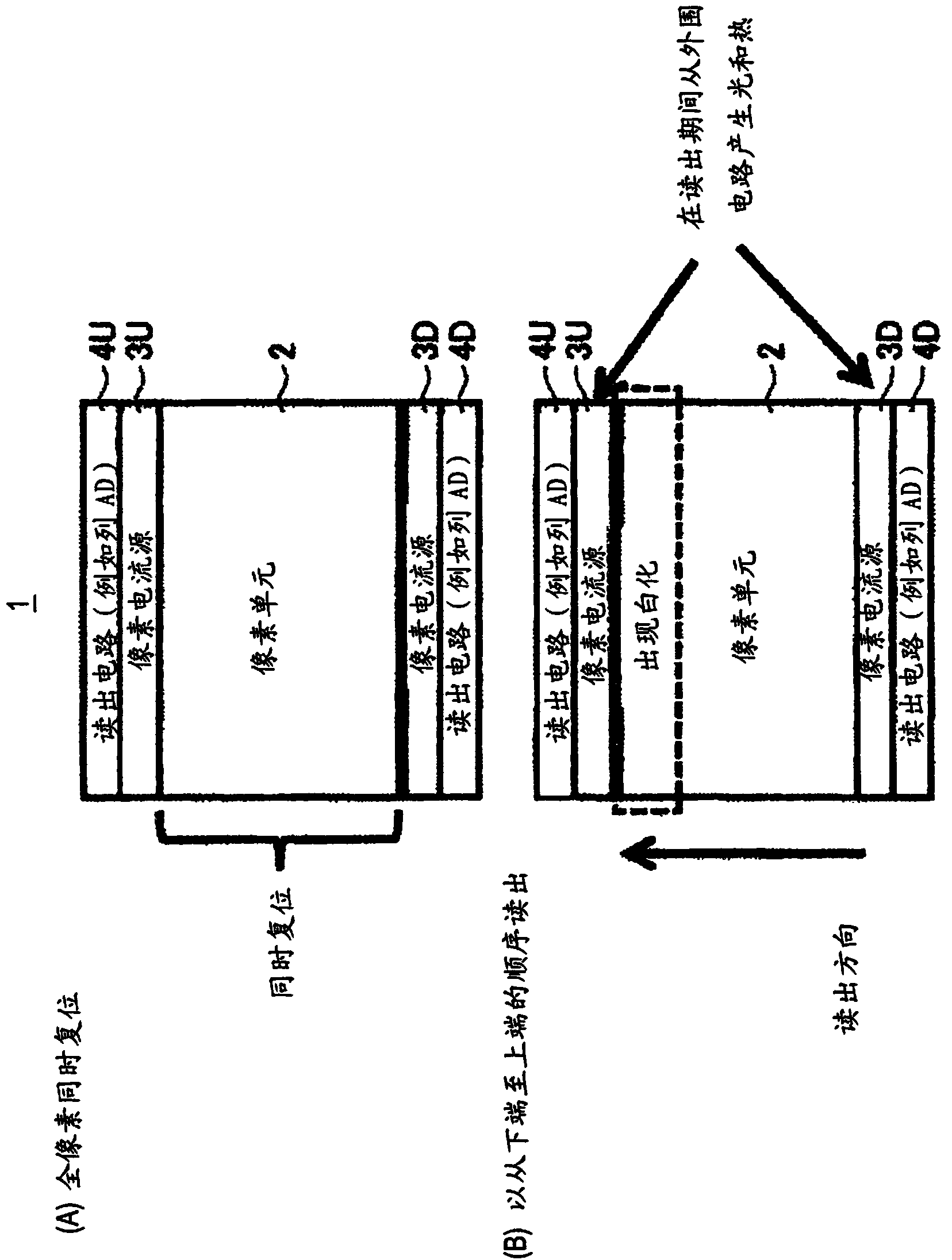
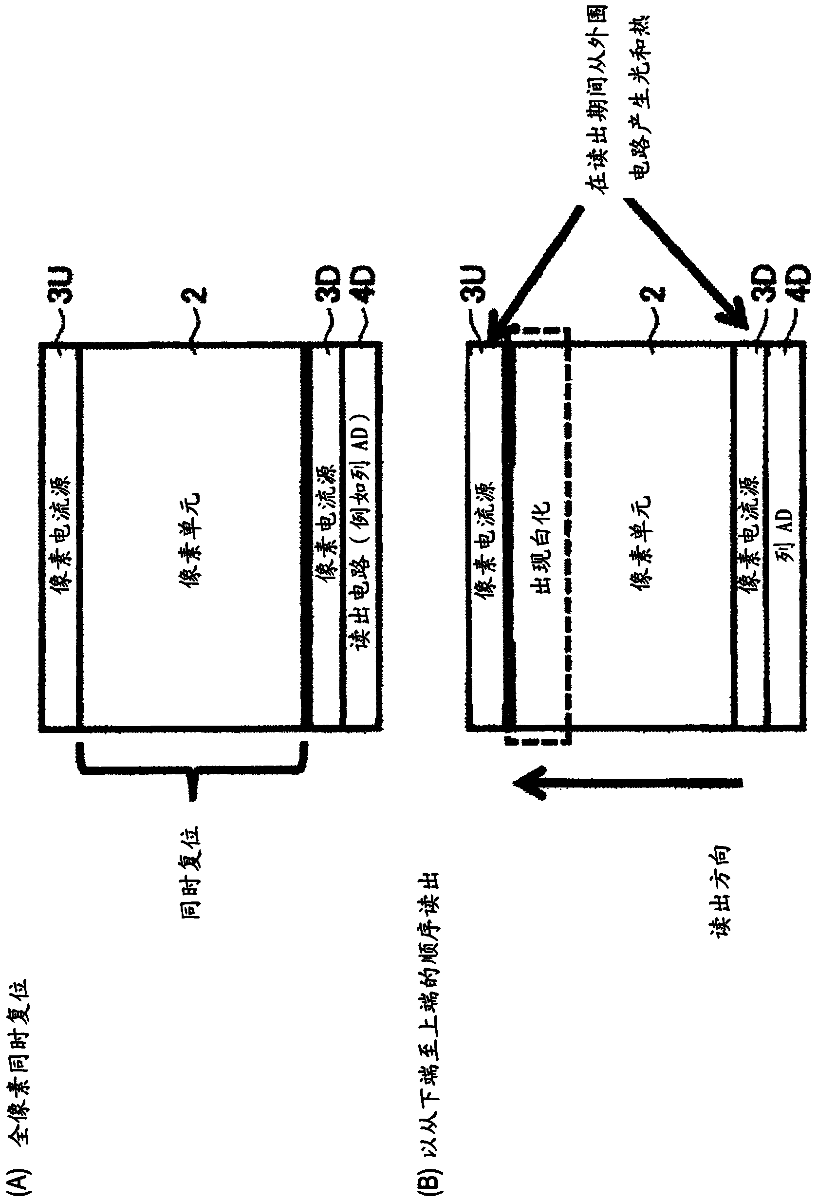
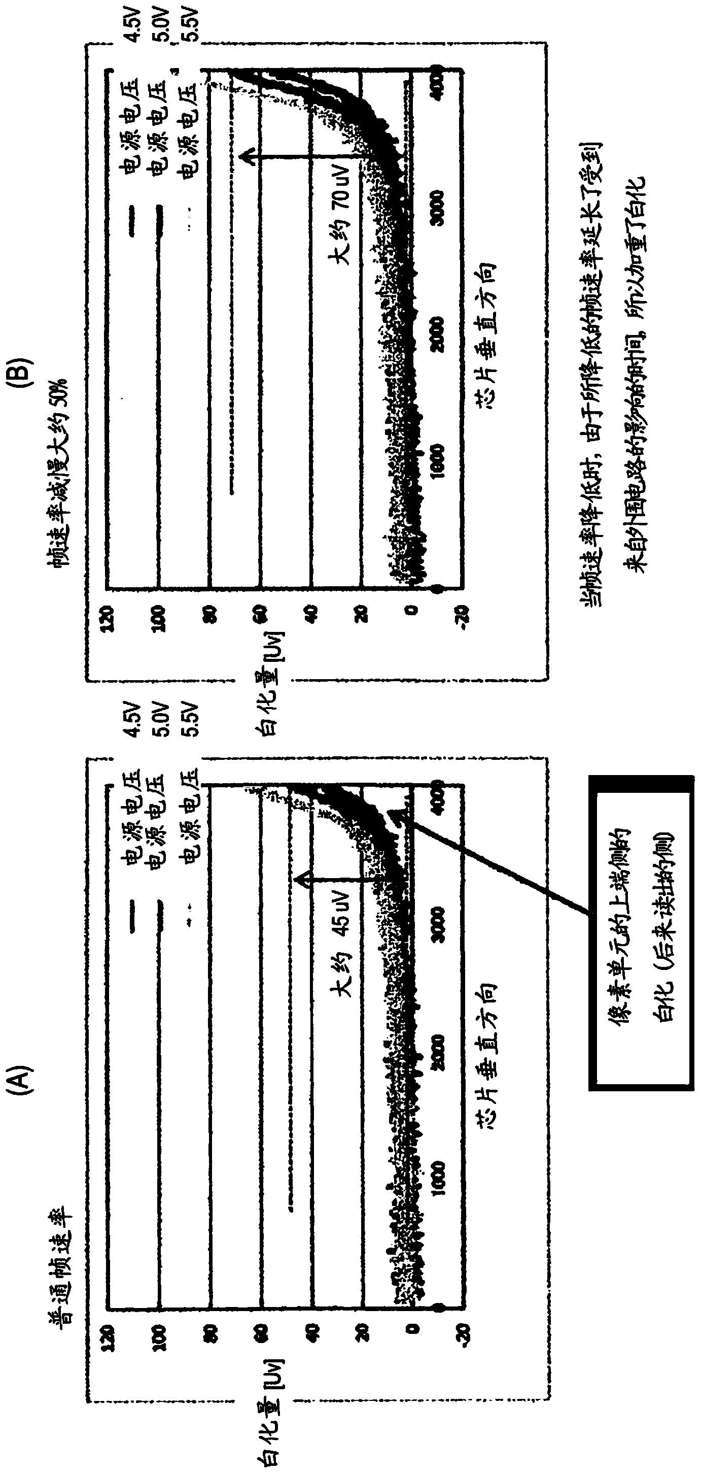
[0143] In the first example, readout is performed in the following order.


PUM


Abstract

The present invention pertains to a solid-state imaging element, a method for driving the element, and a camera system, that enable suppression of white blur at the edge of an image due to the effect of a peripheral circuit. The present invention has: a pixel part in which a plurality of pixels are arranged in a line, the pixel part including a photoelectric conversion element for converting an optical signal to an electrical signal and storing the signal charge, the signal charge being dependent on the exposure time; a peripheral circuit disposed adjacent to an edge portion in a mutually facing arrangement with the pixel part, and driven in association with the read operation of at least a pixel signal; and a pixel-signal read unit for reading the pixel signal from the pixel part in a plurality of pixel units. When the pixel-signal read unit reads all the pixels, all the pixels are reset, and the pixels are then read alternately at least one line at a time starting from at least the lines in a specified region near the peripheral circuit disposed toward the edge portion in a mutually facing arrangement with the pixel part.

Description

technical field [0001] The present invention relates to a solid-state imaging device that performs full-pixel readout, a method of driving the solid-state imaging device, and a camera system. Background technique [0002] In recent years, although image sensors have high resolution, image sensors are still required to image high-quality images at low resolution. [0003] For example, functions such as capturing moving images with digital still cameras and, conversely, imaging still images with video cameras are gaining popularity. [0004] Also, such electronic devices often have a viewfinder for confirming a picture, but the resolution of the viewfinder is generally lower than that of an imaged image. [0005] Also, some digital still cameras and mobile phones incorporate the ability to increase frame rates when imaging at low resolutions in order to image high-speed motion that is conventionally unrecognizable. [0006] As previously described, only one image sensor need...

Claims


Application Information

Patent Timeline
Patent Type & Authority Applications(China)
IPC IPC(8): H04N5/361H01L27/146H04N5/374
CPCH04N5/357H04N5/3456H04N5/378H04N5/374H01L27/14641H04N5/37457H04N5/343H04N5/361H04N25/42H04N25/445H04N25/60H04N25/778H04N25/75H04N25/76
Inventor 辻清茂江口美幸
Owner SONY CORP
Why Eureka
Try Eureka