PCB manufacturing method and PCB

A manufacturing method and printed circuit board technology are applied in the direction of electrical connection formation of printed components, electrical connection of printed components, printed circuit components, etc., which can solve problems such as the inability to meet the requirements of wiring density, and achieve increased wiring space, The effect of enhanced routing capability and increased pad spacing

Active Publication Date: 2014-08-13
NEW H3C TECH CO LTD
View PDF4 Cites 4 Cited by
  • Summary
  • Abstract
  • Description
  • Claims
  • Application Information

AI Technical Summary

Problems solved by technology

[0004] Since the pad spacing between the two crimping holes is fixed, the number of signal lines that can pass through the pad spacing between the two crimping holes is certain. When the wiring density of the PCB is getting higher and higher, obviously, The signal lines that can pass through the pad spacing between the two crimp holes cannot meet the wiring density requirements

Method used


Image

  • PCB manufacturing method and PCB
  • PCB manufacturing method and PCB
  • PCB manufacturing method and PCB

Examples


Embodiment Construction

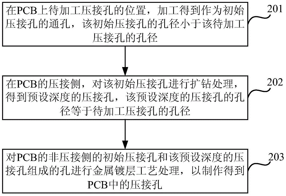
[0028] Aiming at the problems existing in the prior art, the embodiment of the present invention provides a PCB manufacturing method, which is used to make crimping holes in the PCB, such as figure 2 As shown, the method includes the following steps:

[0029] Step 201 , at the position of the crimping hole to be processed on the PCB, a through hole as an initial crimping hole is processed, and the diameter of the initial crimping hole is smaller than that of the crimping hole to be processed.

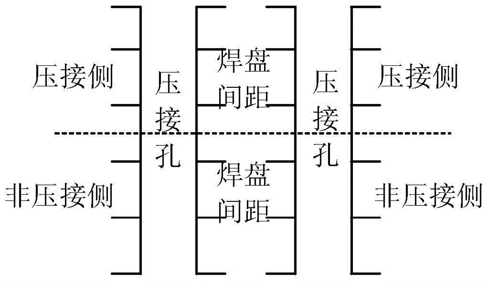
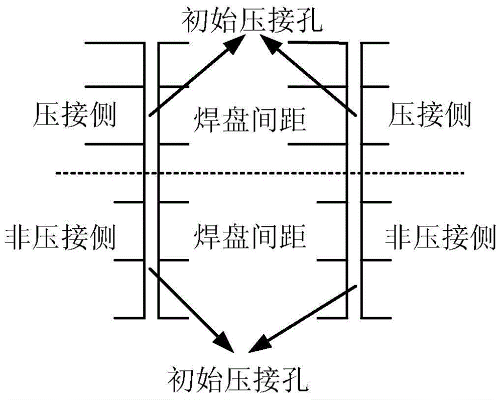
[0030] Wherein, the crimping hole to be processed is the crimping hole that needs to be processed in the prior art. The crimping hole of PCB is divided into crimping side and non-crimping side, such as Figure 3A-Figure 3D As shown, it is a schematic diagram of the processed through hole as the initial crimping hole. The diameter of the initial crimping hole on the crimping side is consistent with the diameter of the initial crimping hole on the non-crimping side, and the initial crim...


PUM


Abstract

The invention discloses a PCB manufacturing method and a PCB. The PCB manufacturing method comprises the steps that through holes serving as initial pressure welding holes are processed in the positions, with pressure welding holes to be processed, on the PCB, wherein the hole diameters of the initial pressure welding holes are smaller than those of the pressure welding holes to be processed; the initial pressure welding holes are counterbored on the pressure welding side of the PCB, pressure welding holes with the preset depth are obtained, and the hole diameters of the pressure welding holes with the preset depth are equal to those of the pressure welding holes to be processed; metal coating fabrication processing is carried out on holes formed by the initial pressure welding holes in the non-pressure-welding side of the PCB and the pressure welding holes with the preset depth so as to obtain pressure welding holes of the PCB. According to the PCB manufacturing method and the PCB, wiring density can be improved, the wiring space of pressure welding pins can be enlarged, and the wiring capacity is enhanced.

Description

technical field [0001] The invention relates to a manufacturing technology of a printed circuit board (PCB), in particular to a PCB manufacturing method and the PCB. Background technique [0002] The technology of connecting the crimping device and PCB (Printed Circuit Board, printed circuit board) by crimping, its working principle is: design crimping pins (ie crimping pins) that can be deformed by force on the crimping device ), when the crimping pin is pressed into the crimping hole of the PCB, the crimping pin is squeezed by the wall of the crimping hole, deformed and attached to the wall of the crimping hole of the PCB, so as to achieve effective connect. [0003] In the existing technology, such as figure 1 As shown, the crimping hole of the PCB is divided into crimping side and non-crimping side. The crimping pin will be pressed into the crimping hole of the crimping side, and the crimping pin will not be pressed into the crimping hole of the non-crimping side. pin...

Claims


Application Information

Patent Timeline
Patent Type & Authority Applications(China)
IPC IPC(8): H05K3/42H05K1/11
Inventor 李义
Owner NEW H3C TECH CO LTD
Why Eureka
Try Eureka