Method and apparatus for uniform electropolishing of damascene ic structures by selective agitation

a damascus ic structure and selective agitation technology, applied in the field of apparatus and methods for surface planarization of metal surfaces, can solve the problems of difficult control of cmp polishing techniques, circuit failure, and inability to use, and achieve the effect of small pore size, easy flow, and sufficient porousness

Inactive Publication Date: 2002-06-20
NOVELLUS SYSTEMS
View PDF0 Cites 66 Cited by
  • Summary
  • Abstract
  • Description
  • Claims
  • Application Information

AI Technical Summary

Benefits of technology

[0018] Electropolishing pads of the invention will be chemically compatible with the electrolyte (i.e. will not dissolve or otherwise break down). The pad will have a small pore size and be sufficiently porous to allow fluid and electrical current to easily flow through. A long-lived pad is also desirable, i.e. one that wears slowly.
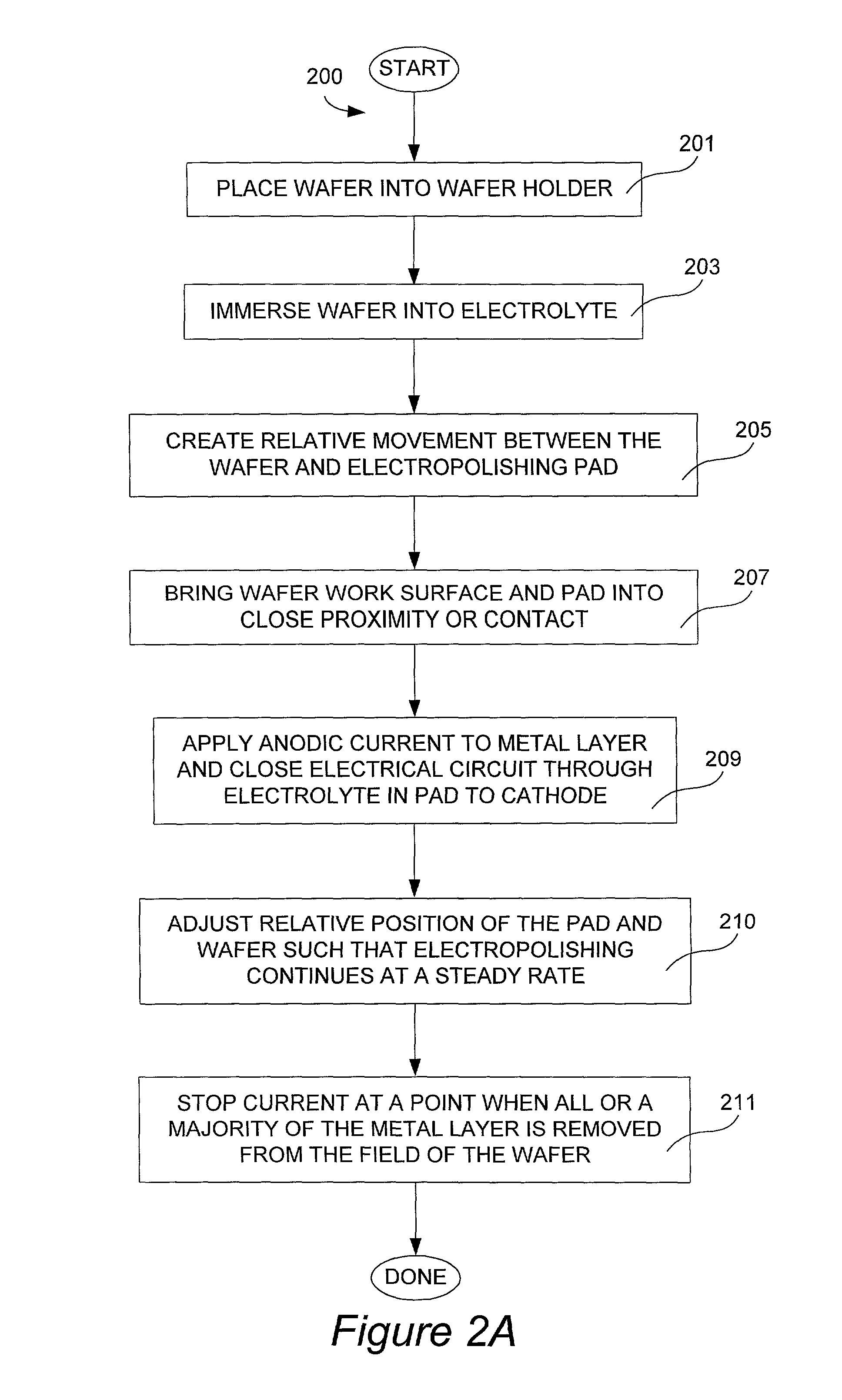
[0019] In some methods, a diffusion barrier material is not added to the surface prior to electropolishing. In these methods the mechanical ability of the pad to thin or remove continually forming anodic surface films from exposed areas leads to an increased current density in those regions. The anodic films are preferentially dissolved away or mechanically removed from the wafer surface, via enhanced agitation of the electrolyte and / or the abrasive structure provided by the electropolishing pad. By selectively removing this film in the exposed regions, substantial differences in current density (and hence removal rate selectivity) is accomplished.
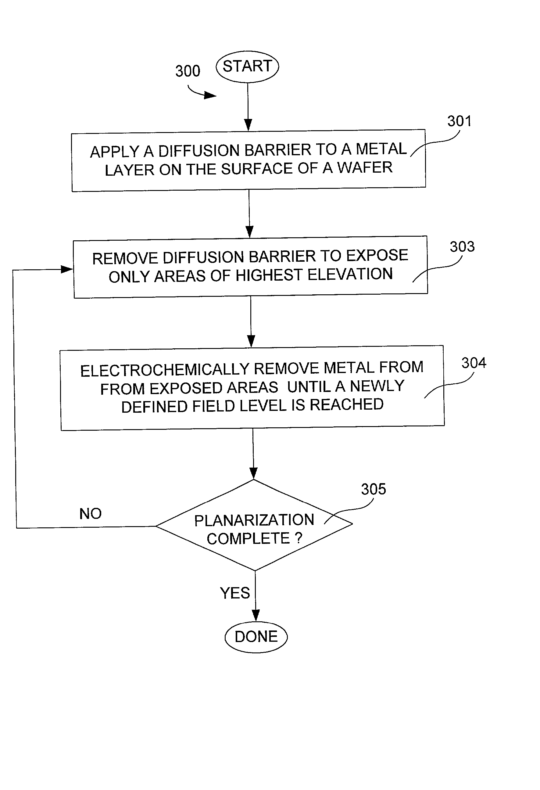
[0021] In a preferred embodiment we add the additional steps of selectively applying a diffusion barrier film to the recesses prior to performing electropolishing with the pad (prior to step (a) above). This process is particularly useful when the properties of the pad and polishing electrolyte are selected to remove diffusion layer material from the recesses more slowly than from the field regions. Any suitable process may be used to apply the diffusion barrier film. Preferably, the diffusion barrier film is applied in a manner that gives it a substantially planar surface. The degree of planarity of the diffusion barrier aids in the uniformity of the subsequent polishing process.

Problems solved by technology

Without planarization, the microscopic canyons that result on the integrated circuit surface from stacking of device features create a topography that (1) would limit the resolution of photo-lithography and creation of dense feature patterns, and (2) would lead to defects in the integrated circuit that would make the circuit unusable.
Unfortunately, CMP polishing techniques are difficult to control; the endpoint can be difficult to detect.
They are also expensive.
The high equipment cost, waste handling cost, and low throughput contribute to the overall expense of CMP.
Also, with the introduction of low-k dielectrics into chip production, modification of traditional CMP processes will be required, as current methods result in cracking and delamination of most low-k materials, which have a very low compression strength, and are extremely fragile.
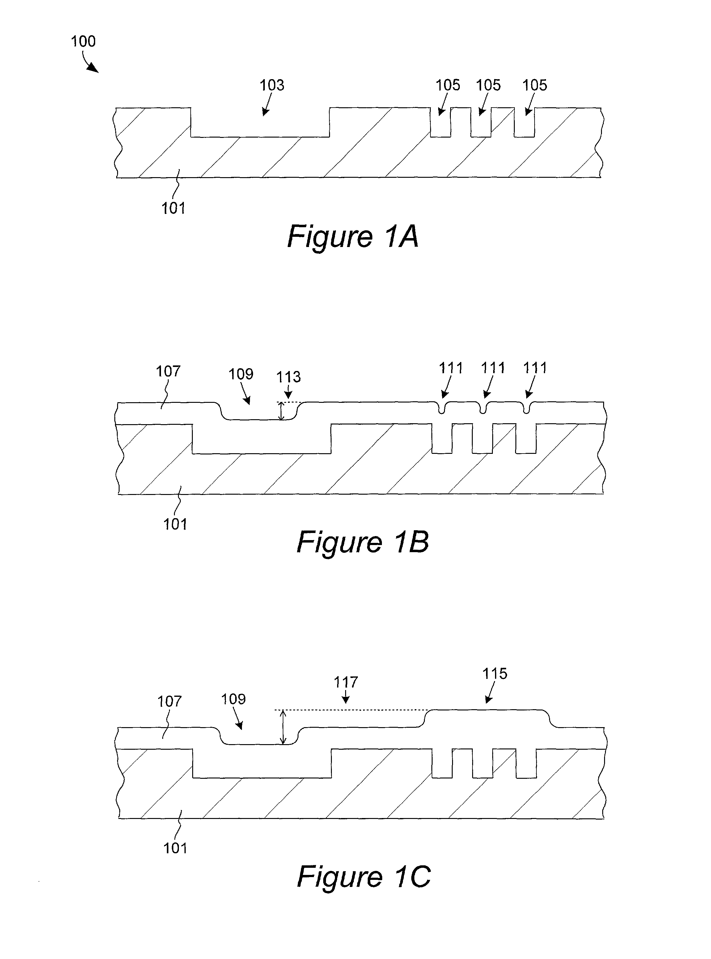
A problem arises during the electropolishing of surfaces in which a large number of low aspect ratio (larger width than depth) features exist.
To do so would be uneconomical due to necessary removal of the large excess of metal at a later stage.
Obviously, this is an unacceptable result.
The current state of electropolishing technology has additional difficulties.
While these baths are effective in achieving good polishing and planarization rates, they make it difficult to remove defect-causing bubbles and to handle the fluids in general.
The hydrogen can become entrained in the electrolyte, complicating tool design and presenting a potential safety hazard.
In addition, these baths also have high resistivities, making for large power requirements and substantial amounts of generated heat (which must be removed to maintain a constant process control).
While this technique is more effective with respect to conventional electropolishing approaches, the added application step can add cost to the operation, and may not sufficiently address planarization of raised regions (bumps) on the metal surface.
Thus, use of advanced "bottom up" electrofill paradigms in combination with wafers having many low and high aspect features have created a problem of deposited metal surfaces having a range of topography to be planarized that is unusually large, i.e. containing both recessed and raised areas.
Therefore, while electroplating is a preferred method of metalization, various aspects of improved plating regimens create challenging topography for subsequent planarization.

Method used


Image

  • Method and apparatus for uniform electropolishing of damascene ic structures by selective agitation
  • Method and apparatus for uniform electropolishing of damascene ic structures by selective agitation
  • Method and apparatus for uniform electropolishing of damascene ic structures by selective agitation

Examples


Embodiment Construction

[0032] In the following detailed description of the present invention, numerous specific embodiments are set forth in order to provide a thorough understanding of the invention. However, as will be apparent to those skilled in the art, the present invention may be practiced without these specific details or by using alternate elements or processes. For example, the invention is described in terms of methods and apparatus in relation to electroplanarization of a metal layer for semiconductor wafer processing. The invention is not limited to semiconductor wafer processing, that is, the invention can be used to planarize metal surfaces on other substrates as well. In some descriptions herein, well-known processes, procedures, and components have not been described in detail so as not to unnecessarily obscure aspects of the present invention.

[0033] The invention is primarily described in terms of electropolishing; however, it is critical to understand that the methods and apparatus desc...


PUM

PropertyMeasurementUnit
diameteraaaaaaaaaa
diameteraaaaaaaaaa
weight percentaaaaaaaaaa

Abstract

The present invention pertains to apparatus and methods for planarization of metal surfaces having both recessed and raised features, over a large range of feature sizes. The invention accomplishes this by increasing the fluid agitation in raised regions with respect to recessed regions. That is, the agitation of the electropolishing bath fluid is agitated or exchanged as a function of elevation on the metal film profile. The higher the elevation, the greater the movement or exchange rate of bath fluid. In preferred methods of the invention, this agitation is achieved through the use of a microporous electropolishing pad that moves over (either near or in contact with) the surface of the wafer during the electropolishing process. Thus, methods of the invention are electropolishing methods, which in some cases include mechanical polishing elements.

Description

CROSS-REFERENCE TO RELATED APPLICATIONS[0001] This application is a continuation-in-part claiming priority under 35 USC .sctn.120 from U.S. patent application Ser. No. 09 / 412,837 filed Oct. 5, 1999, naming Mayer et al. as inventors, and titled "Electroplanarization of Large and Small Damascene Features Using Diffusion Barriers and Electropolishing," which claims priority under 35 USC .sctn.119(e) from provisional patent application No. 60 / 105,700. Both of these applications are incorporated herein by reference in their entireties for all purposes.FIELD OF THE INVENTION[0002] The present invention pertains to apparatus and methods for surface planarization of metal surfaces. More specifically, it relates to electropolishing, electroetching and chemical etching technology for planarizing metal surfaces having low aspect ratio recesses or trenches as well as raised regions (bumps).BACKGROUND OF THE INVENTION[0003] In the fabrication of integrated circuits, as the number of levels in an...

Claims


Application Information

Patent Timeline
Patent Type & Authority Applications(United States)
IPC IPC(8): B23H5/08H01L21/321H01L21/3213
CPCB23H5/08H01L21/32115H01L21/3212H01L21/32134
Inventor MAYER, STEVEN T.CONTOLINI, ROBERT J.BROADBENT, ELIOT K.DREWERY, JOHN S.
Owner NOVELLUS SYSTEMS
Why Eureka
Try Eureka