High aspect ratio stacked MLCC design
A high aspect ratio, multi-layer ceramic technology, applied in the field of improved external lead design, high integration density electronic components, can solve the problems of easy dumping, increased aspect ratio, etc.
- Summary
- Abstract
- Description
- Claims
- Application Information
AI Technical Summary
Problems solved by technology
Method used
Image

Examples
Embodiment Construction
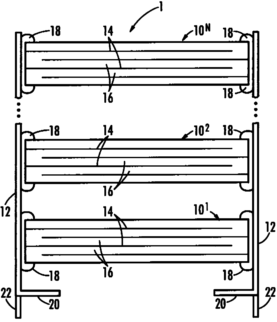
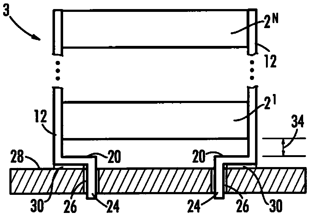
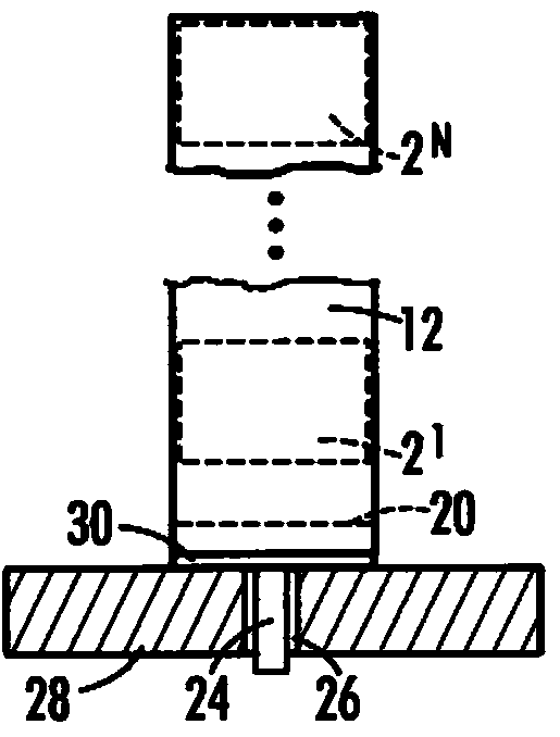
[0040] The present invention is directed to an improved lead structure for stacked electronic components, in particular to stacked MLCCs. More specifically, the present invention is directed to lead structures that include positioning pins that allow for aspect ratios such as Figure 25 The height (H) to shortest width (W) ratio shown is very large while minimizing the possibility of the stacked components shifting or toppling during handling.
[0041] The present invention provides a capacitor stack, most preferably an MLCC capacitor stack, that allows the designer to take advantage of the vertical space on the board to increase the density of capacitors in a given area of the board, thereby enhancing functionality such as capacitance density. This is accomplished by incorporating into the leadframe stabilizing feet designed for surface mount applications, where the stabilizing feet extend into the void and preferably through the substrate or board, while the leadframe pins...
PUM
 Abstract
Description
Claims
Application Information
PatSnap Eureka turns technology decisions into work you can execute. Powered by our Innovation Knowledge Graph, it runs expert workflows across engineering, life sciences, materials and intellectual property. Get your review-ready output in minutes.


