Array substrate and preparing method thereof as well as capacitance embedding touch screen

A technology of array substrates and conductive wires, applied in the fields of electrical digital data processing, instruments, calculations, etc., can solve problems such as large impedance, signal delay, and impact on touch screen performance, so as to improve touch performance, avoid signal delay, and reduce production costs Effect

Inactive Publication Date: 2014-09-17
BOE TECH GRP CO LTD +1
View PDF8 Cites 9 Cited by
  • Summary
  • Abstract
  • Description
  • Claims
  • Application Information

AI Technical Summary

Problems solved by technology

Due to the high resistance of ITO itself and the thin ITO layer during actual deposition, the Rx and Tx made of ITO usually have large impedances. When the touch part and the display part are driven in time, it is easy to cause signal delay and affect Touch Screen Performance

Method used


Image

  • Array substrate and preparing method thereof as well as capacitance embedding touch screen
  • Array substrate and preparing method thereof as well as capacitance embedding touch screen
  • Array substrate and preparing method thereof as well as capacitance embedding touch screen

Examples


Embodiment 1

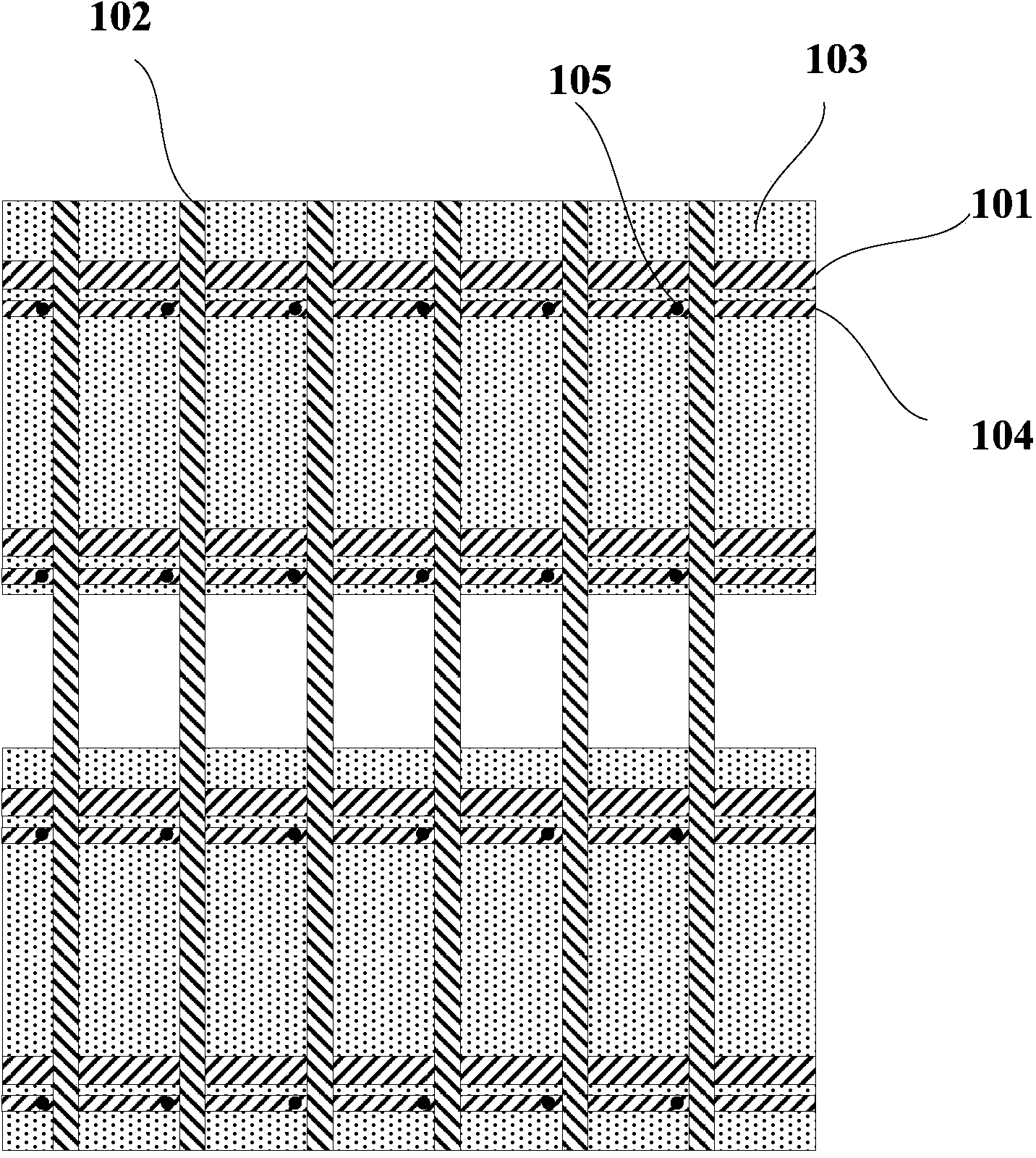
[0041] Please refer to figure 1 , figure 1 It is a schematic structural diagram of the array substrate according to Embodiment 1 of the present invention.

[0042] The array substrate comprises: a gate line layer comprising a plurality of gate lines 101 arranged in parallel, a data line layer comprising a plurality of data lines 102 arranged in parallel, and a touch driving electrode layer comprising a plurality of touch driving electrodes 103 arranged in parallel , wherein, the gate lines 101 and the data lines 102 are vertically crossed, and the touch driving electrodes 103 are parallel to the gate lines 101 .

[0043] In order to avoid the signal delay of the touch driving electrodes 103, the array substrate further includes: a first conductive line 104 provided on the same layer and with the same material as the gate line 101, the first conductive line 104 is arranged in parallel with the gate line 101, That is, it is also arranged parallel to the touch driving electrode...

Embodiment 2

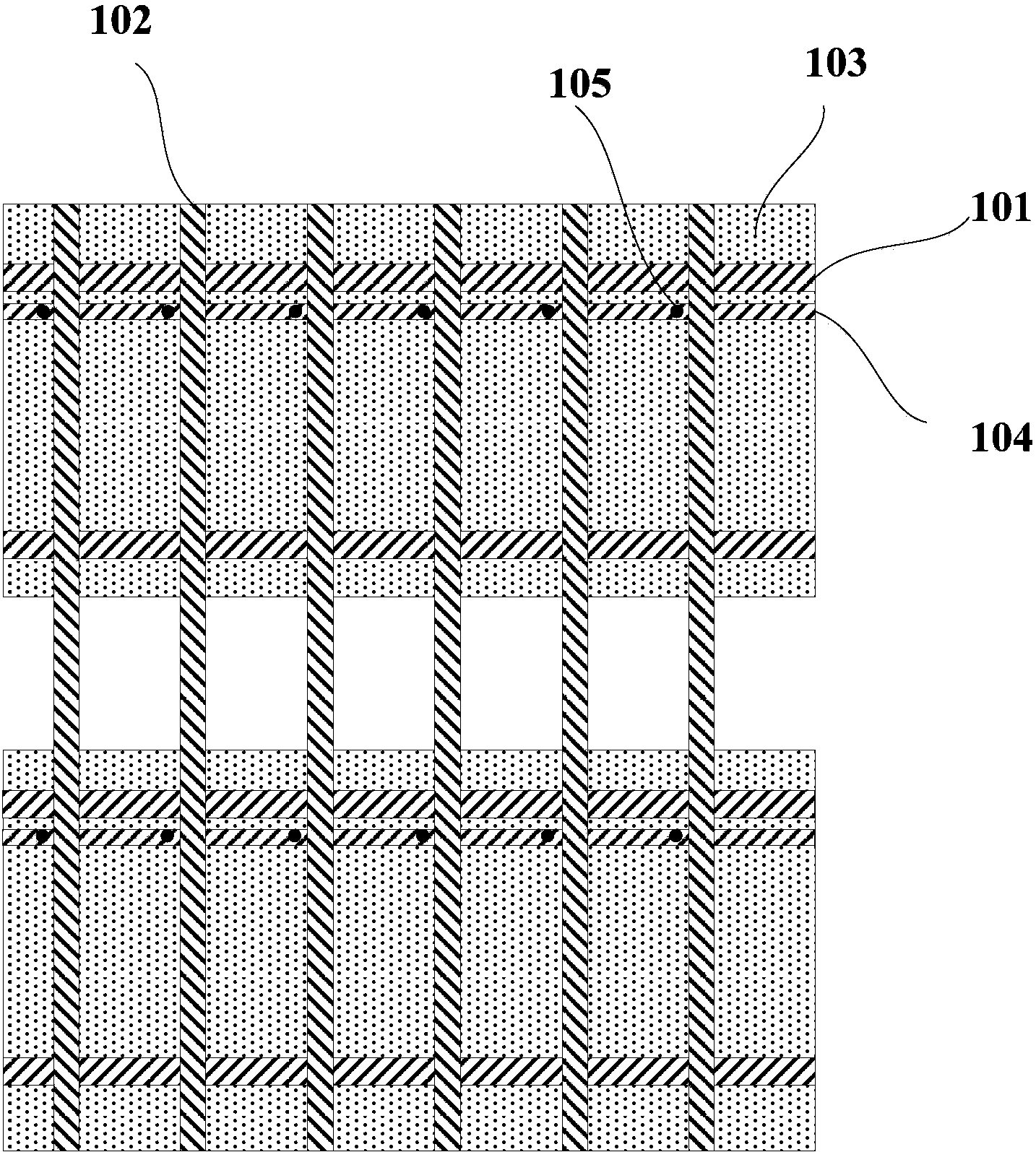
[0046] When the gate lines 101 are made of opaque metal, the first conductive lines 104 are also made of opaque metal. In order not to affect the aperture ratio of the display panel, the number of the first conductive lines 104 can be appropriately reduced. Please refer to figure 2 , figure 2 It is a schematic structural diagram of the array substrate of Embodiment 2 of the present invention. Compared with Embodiment 1, this embodiment differs in that a touch driving electrode 103 is configured with a first conductive line 104 connected in parallel thereto.

Embodiment 3

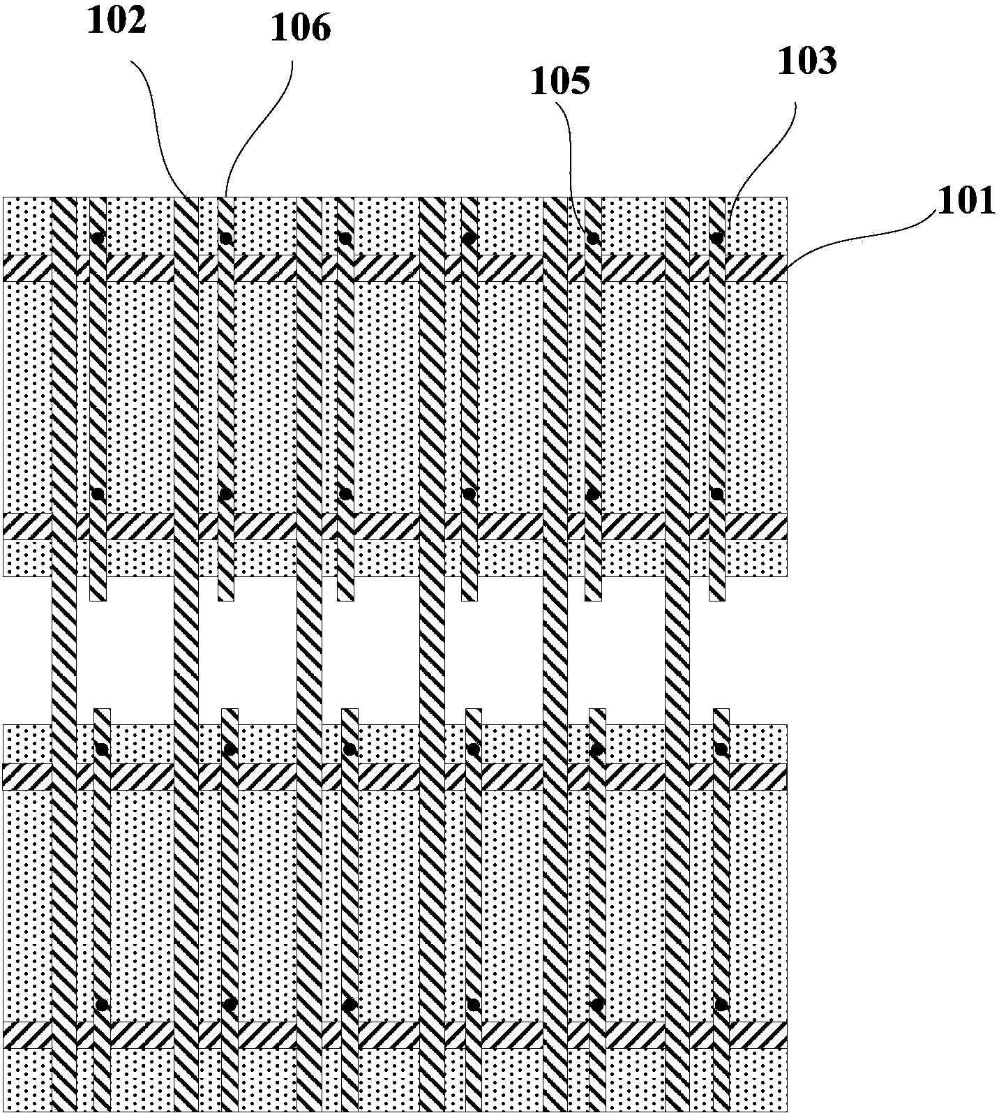
[0048] Please refer to image 3 , image 3 It is a schematic structural diagram of the array substrate according to Embodiment 3 of the present invention.

[0049] The array substrate comprises: a gate line layer comprising a plurality of gate lines 101 arranged in parallel, a data line layer comprising a plurality of data lines 102 arranged in parallel, and a touch driving electrode layer comprising a plurality of touch driving electrodes 103 arranged in parallel , wherein the gate line 101 and the data line 102 are vertically intersected, and the touch driving electrode 103 is parallel to the gate line 101 and perpendicular to the data line 102 .

[0050] In order to avoid the signal delay of the touch driving electrodes 103, the array substrate further includes: a third conductive line 106 arranged in the same layer and the same material as the data line 102, the third conductive line 106 is arranged in parallel with the data line 102, That is, it is vertically arranged w...


PUM


Abstract

The invention provides an array substrate and a preparing method thereof as well as a capacitance embedding touch screen. The array substrate comprises an signal wire layer and a touch control electrode layer; the signal wire layer comprises multiple parallel signal wires; the touch control electrode layer comprises multiple touch control electrodes in parallel arrangement; the array substrate also comprises electric conduction wires; the electric conduction wires and the signal wires of the array substrate are made of the same material and on the same layer; all or part of the touch control electrodes are connected with the electric conduction wires in parallel. According to the array substrate and the preparing method thereof as well as the capacitance embedding touch screen, the electric conduction wires connected with the touch control electrodes are arranged on the array substrate, so the signal delay of the touch electrodes is avoided as much as possible; the touch control performance is improved, and the electric conduction wires and the signal wires of the array substrate are made of the same material and on the same layer, so the production cost and the yield risk in the production process are reduced as much as possible.

Description

technical field [0001] The invention relates to the field of display technology, in particular to an array substrate, a preparation method thereof, and a capacitive embedded touch screen. Background technique [0002] Capacitive touch screen has become the current mainstream touch screen due to its thinner, higher light transmittance, stronger stability, and support for multi-touch. Among them, the in-cell mode can make the capacitive touch screen thinner and have higher light transmittance. However, since the touch part and the display part of the capacitive touch screen often need time-sharing driving, signal delay (loading) becomes an important factor restricting the performance of touch control and display. [0003] The capacitive in-cell touch screen includes a touch driving electrode layer and a touch sensing electrode layer that usually include insulation. The touch driving electrode layer includes a plurality of touch driving electrodes TX, and the touch sensing ele...

Claims


Application Information

Patent Timeline
Patent Type & Authority Applications(China)
IPC IPC(8): G06F3/044G02F1/1333
CPCG02F1/1333G06F3/0446G06F3/0443
Inventor 龙跃高永益黄炜赟王杨
Owner BOE TECH GRP CO LTD
Why Eureka
Try Eureka