Opto-electronic integrated circuit device, opto-electronic integrated circuit system and transmission method

an optoelectronic integrated circuit and integrated circuit technology, applied in the direction of instruments, electromagnetic repeaters, optical elements, etc., can solve the problems of system bulkiness and large delay of signals, and achieve the effect of preventing signal delay, preventing transmission speed decrease, and small siz

Inactive Publication Date: 2007-05-29
FUJITSU SEMICON LTD
View PDF11 Cites 9 Cited by
  • Summary
  • Abstract
  • Description
  • Claims
  • Application Information

AI Technical Summary

Benefits of technology

[0013]An object of the present invention is to provide an opto-electronic integrated circuit device which, even when an optical signal is transmitted between a number of the opto-electronic integrated circuit devices, the delay of the signal can be prevented, and which can be downsized; an opto-electronic integrated circuit system using the opto-electronic integrated circuit device; and a transmission method using three opto-electronic integrated circuit device system.
[0018]According to the present invention, when an optical signal inputted to one opto-electronic integrated circuit device is to be processed by said one opto-electronic integrated circuit the optical signal has been inputted to, the inputted optical signal can be converted to an electric signal and inputted to the semiconductor chip or others. When the inputted optical signal is to be processed by another opto-electronic integrated circuit device, the optical switch is changed over, and the inputted optical signal can be transmitted as it is to said another opto-electronic integrated circuit device. Thus, according to the present invention, a number of the optical waveguides, the electric-optic conversion elements and the opto-electric conversion elements are not necessary, which allows the opto-electronic integrated circuit system to be small sized. Furthermore, when an optical signal is to be processed by said another opto-electronic integrated circuit device, the optical signal is not converted to an electric signal and from the electric signal by the opto-electronic integrated circuit device the optical signal has been inputted to, which can prevent the decrease of the transmission speed. Thus, according to the present invention, even when an optical signal is transmitted between a large number of opto-electronic integrated circuit devices, the delay of the signal can be prevented, and the opto-electronic integrated circuit system can be small-sized.
[0020]According to the present invention, when an optical signal inputted to an opto-electronic integrated circuit is to be processed by another opto-electronic integrated circuit, the opto-electronic integrated circuit the optical signal has been inputted to need not convert the optical signal to an electric signal or the electric signal to the optical signal, which can decrease the load of the processing of the opto-electronic integrated circuit devices to be decreased.
[0021]According to the present invention, when an optical signal inputted to an opto-electronic integrated circuit is to be processed by another opto-electronic integrated circuit, the opto-electronic integrated circuit device the optical signal has been inputted to does not convert the optical signal to an electric signal and the electric signal to the optical signal, which can decrease the electric power consumption.

Problems solved by technology

Accordingly, it is not easy to form a system which enables the transmission of optical signals among a number of opto-electronic integrated circuit devices, and even when such system is formed, the system will be bulky.
Accordingly, when an optical signal is transmitted via a number of the opto-electronic integrated circuit devices, the delay of the signal is very large.

Method used


Image

  • Opto-electronic integrated circuit device, opto-electronic integrated circuit system and transmission method
  • Opto-electronic integrated circuit device, opto-electronic integrated circuit system and transmission method
  • Opto-electronic integrated circuit device, opto-electronic integrated circuit system and transmission method

Examples


Embodiment Construction

[0026][An Embodiment]

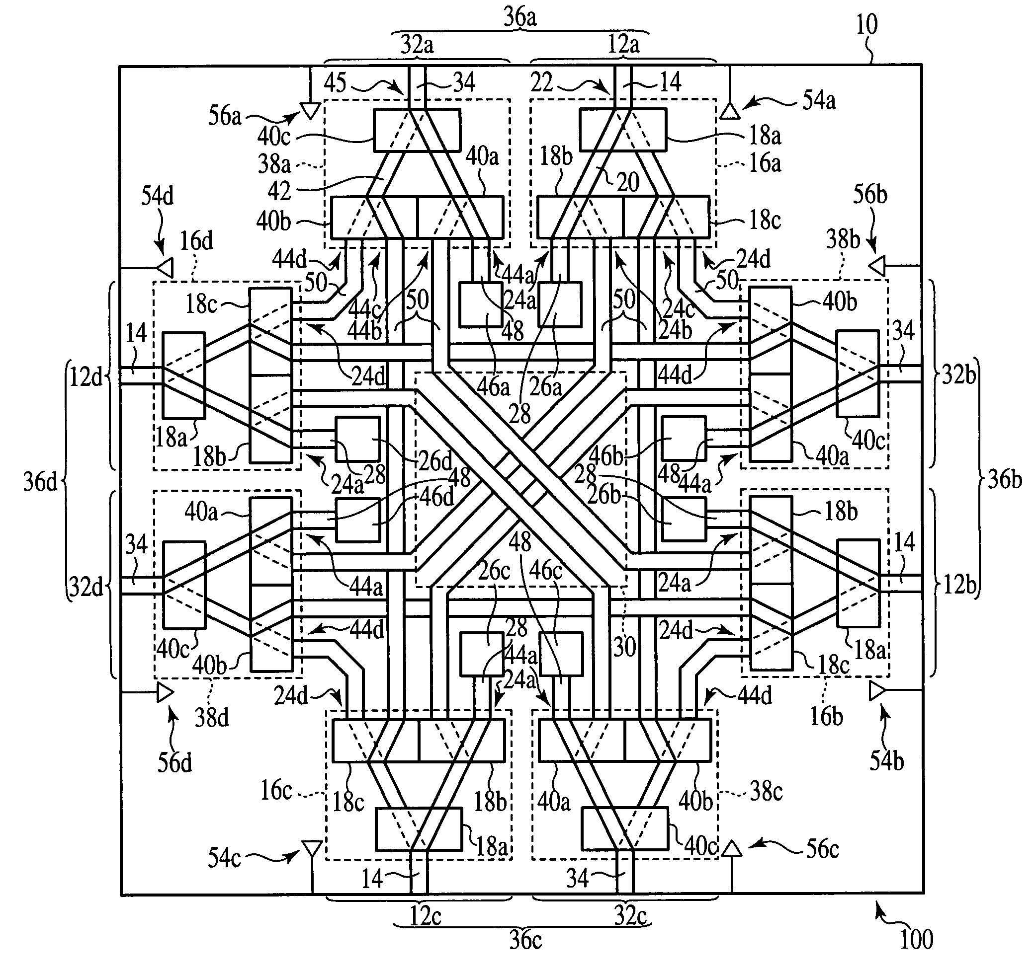
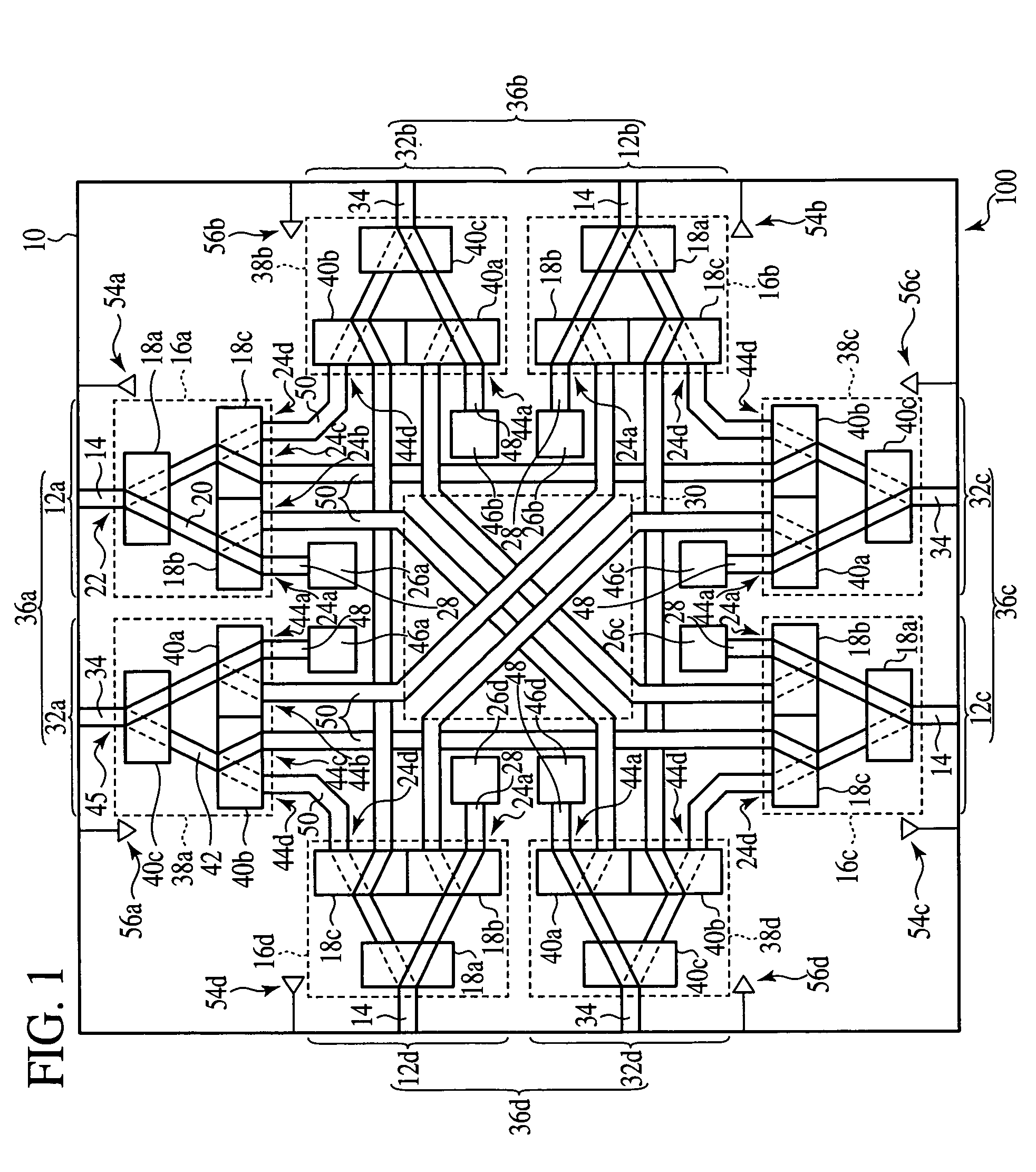
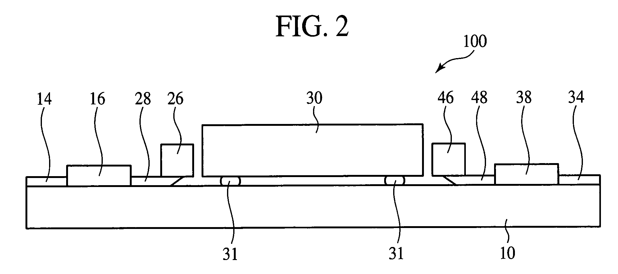
[0027]An opto-electronic integrated circuit device, an opto-electronic integrated circuit system and a transmission method according to one embodiment of the present invention will be explained with reference to FIGS. 1 to 4. FIG. 1 is a plan view of the opto-electronic integrated circuit device according to the present embodiment. FIG. 2 is a sectional view of the opto-electronic integrated circuit device according to the present embodiment. FIG. 3 is a circuit diagram of a part of the opto-electronic integrated circuit device according to the present embodiment.

[0028](The Opto-Electronic Integrated Circuit Device)

[0029]As illustrated, optical waveguides 14 are provided respectively in input ports 12a–12d on a substrate 10. The substrate 10 is, e.g., a silicon substrate, a ceramic substrate, a resin substrate (printed circuit board) or others. The optical waveguides 14 are for inputting optical signals from the outside.

[0030]Optical signal input parts 16a–16d a...


PUM


Abstract

The opto-electronic integrated circuit device comprises an optical switch 18 provided in an input port 12a of a first input / output port 36a over a substrate 10 and changing over an optical path of an optical signal inputted from the input port 12a and outputting the optical signal through one of a plurality of output terminals 24a–24d; an opto-electric conversion element 26a optically connected to one of the plural output terminals of the optical switch 18, and converting the optical signal outputted from one of the output terminals 24a–24d of the optical switch 18 to an electric signal and inputting the converted electric signal in a semiconductor element 30 mounted over the substrate 10; and an optical waveguide 50 optically connected to another of the plural output terminal 24d of the optical switch 18 and outputting the optical signal outputted from said another output terminal 24d of the optical switch 18 through an output port 32b of a second input / output port 36b over the substrate 10.

Description

CROSS-REFERENCE TO RELATED APPLICATION[0001]This application is based upon and claims priority of Japanese Patent Application No. 2004-51131, filed on Feb. 26, 2004, the contents being incorporated herein by reference.BACKGROUND OF THE INVENTION[0002]The present invention relates to an opto-electronic integrated circuit device, an opto-electronic integrated circuit system and a transmission method using the opto-electronic integrated circuit system.[0003]Recently, opto-electronic integrated circuit devices each including optical elements and electronic devices integrated on a substrates are proposed. In the proposed opto-electronic integrated circuit device, the elements for converting electric signals to optical signals are, e.g., laser diodes, etc., and the elements for converting optical signals to electric signals are, e.g., photodiodes, etc. The optical elements are interconnected by optical fibers, etc., and the electronic devices are interconnected by electric interconnection...

Claims


Application Information

Patent Timeline
Patent Type & Authority Patents(United States)
IPC IPC(8): G02B6/12G02B6/42G02B6/122H01L31/12H04B10/27H04B10/29H04B10/80H04J14/02H04Q11/00
CPCH04Q11/0005H04Q2011/0058H01L2224/16225B26D7/1818B26F1/40
Inventor HOSHINO, MASATAKASATO, TOMOTOSHI
Owner FUJITSU SEMICON LTD
Why Eureka
Try Eureka