Liquid crystal display and manufacturing method thereof

a technology of liquid crystal display and manufacturing method, which is applied in the field of liquid crystal display, can solve the problems of increasing manufacturing cost associated therewith and delay of signal applied to the common electrode, and achieve the effect of preventing signal delay of the common electrode and increasing manufacturing cos

Active Publication Date: 2014-09-18
SAMSUNG DISPLAY CO LTD
View PDF0 Cites 8 Cited by
  • Summary
  • Abstract
  • Description
  • Claims
  • Application Information

AI Technical Summary

Benefits of technology

[0032]According to the liquid crystal display and the manufacturing method according to an exemplary embodiment of the present invention, the increase of the manufacturing cost and the signal delay of the common electrode may be prevented while forming two field generating electrodes on one substrate.

Problems solved by technology

The liquid crystal display has certain benefits in that it is may be readily manufactured having a light weight and thin formation t. However, there may also be certain difficulties associated with a liquid crystal display such as, for example, that lateral visibility may be lower than front visibility.
When forming two field generating electrodes on one display panel, to respectively form the field generating electrodes, different photomasks may be required which may thereby result in an increase in the manufacturing costs associated therewith.
Also, when connecting the common electrodes applied with a voltage of a constant magnitude, a signal applied to the common electrode may be delayed.

Method used


Image

  • Liquid crystal display and manufacturing method thereof
  • Liquid crystal display and manufacturing method thereof
  • Liquid crystal display and manufacturing method thereof

Examples


Embodiment Construction

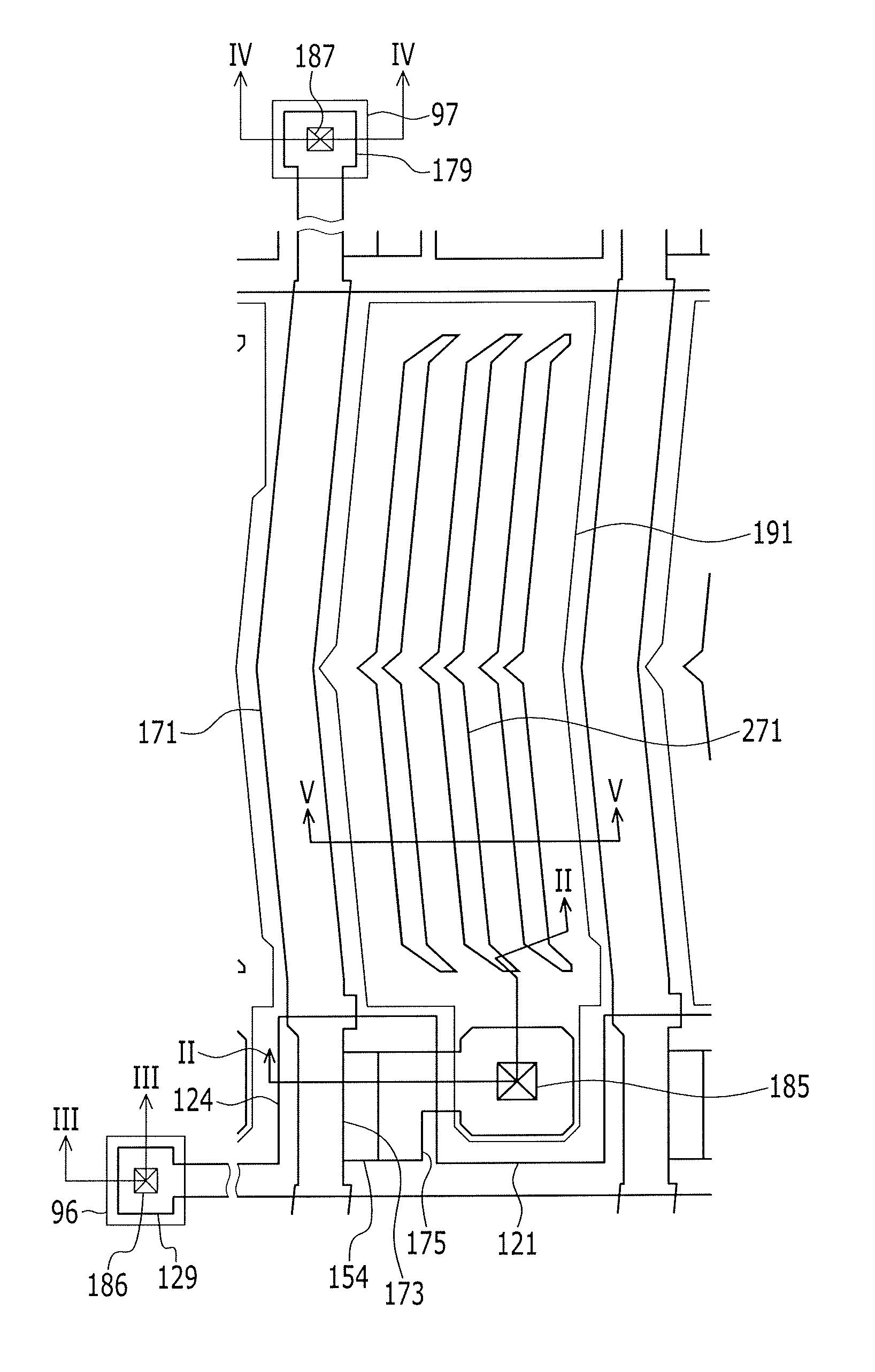
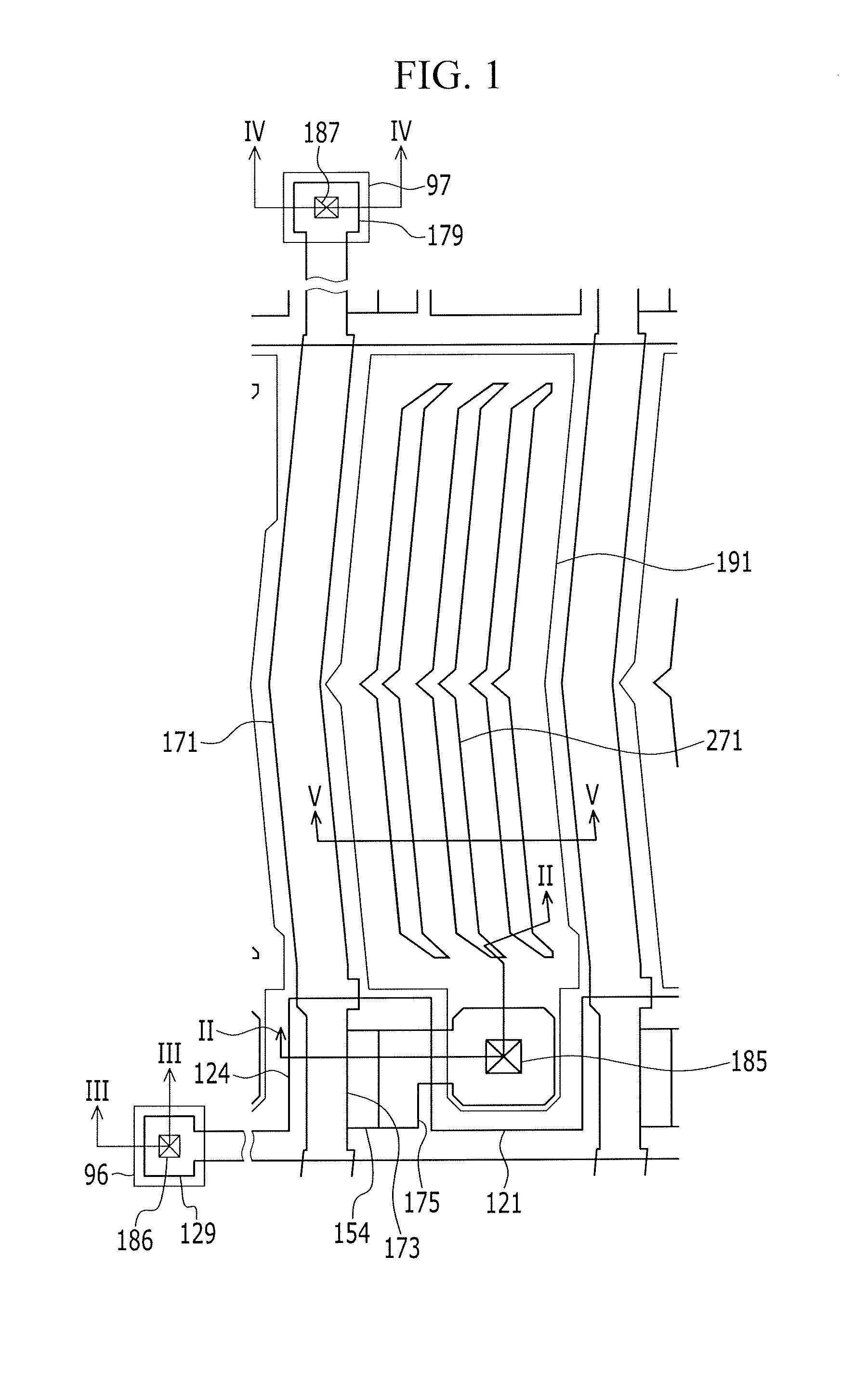
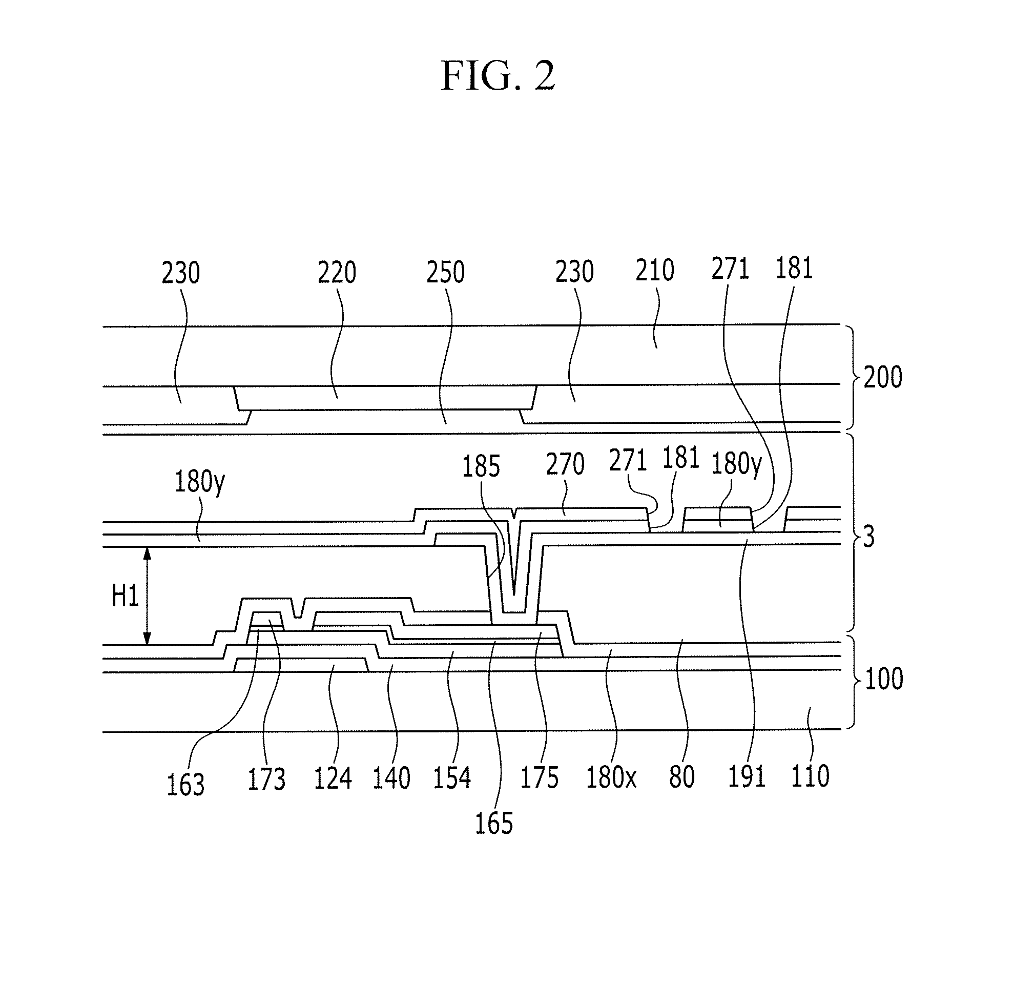
[0048]Exemplary embodiments of the present invention will be described more fully hereinafter with reference to the accompanying drawings, in which exemplary embodiments of the invention are shown.

[0049]In the drawings, the thickness of layers, films, panels, regions, etc., may be exaggerated for clarity. Like reference numerals designate like elements throughout the specification. It will be understood that when an element such as a layer, film, region, or substrate is referred to as being “on” another element, it can be directly on the other element or intervening elements may also be present.

[0050]As used herein, the singular forms, “a”, “an”, and “the” are intended to include plural forms as well, unless the context clearly indicates otherwise.

[0051]Now, a liquid crystal display according to an exemplary embodiment of the present invention will be described with reference to the drawings.

[0052]Firstly, a liquid crystal display according to an exemplary embodiment of the present ...


PUM

PropertyMeasurementUnit
angleaaaaaaaaaa
angleaaaaaaaaaa
angleaaaaaaaaaa

Abstract

A liquid crystal display includes a first substrate, gate lines and data lines disposed on a display area of the first substrate, a common voltage line disposed on a peripheral area of the first substrate, a common voltage transmission unit extending from the common voltage line, an organic layer disposed on the common voltage transmission unit and the common voltage line, a connecting member disposed on the organic layer disposed on the peripheral area, a first insulating layer disposed on the pixel electrode and the connecting member, a common electrode disposed on the first insulating layer, and a short point connecting the connecting member and the common electrode to each other. The common electrode and the first insulating layer include a plurality of cutouts in the peripheral region and display region of the first substrate which have substantially a same plane shape as each other.

Description

CROSS-REFERENCE TO RELATED APPLICATION[0001]This application claims priority to Korean Patent Application No. 10-2013-0027893 filed on Mar. 15, 2013, the disclosure of which is hereby incorporated by reference herein in its entirety.(a) TECHNICAL FIELD[0002]The present disclosure relates to a liquid crystal display and a manufacturing method thereof.(b) DISCUSSION OF THE RELATED ART[0003]Liquid crystal displays (LCDs) are one of the most widely used flat panel displays, and they display images by applying voltages to field-generating electrodes to generate an electric field in a liquid crystal (LC) layer that determines orientations of LC molecules therein to adjust polarization of incident light.[0004]The liquid crystal display has certain benefits in that it is may be readily manufactured having a light weight and thin formation t. However, there may also be certain difficulties associated with a liquid crystal display such as, for example, that lateral visibility may be lower tha...

Claims


Application Information

Patent Timeline
Patent Type & Authority Applications(United States)
IPC IPC(8): G02F1/1345
CPCG02F1/1345G02F1/13458G02F1/1362G02F1/13452G02F1/1368G02F1/1343G02F1/13454G02F1/1341
Inventor KIM, SUNG MANKWON, YEONG-KEUNKIM, DUK-SUNGSONG, MIN-CHULLEE, EU GENECHAE, SOO JUNG
Owner SAMSUNG DISPLAY CO LTD
Why Eureka
Try Eureka