Pixel circuit, driving method of pixel circuit and display device of pixel circuit

A technology for pixel circuits and driving levels, applied in the field of pixel circuits and their driving methods and display devices, capable of solving the problems of incomplete compensation of driving levels and slow charging, etc., achieving the effect of compensating driving levels and improving compensation effects

Active Publication Date: 2014-10-01
BOE TECH GRP CO LTD
View PDF5 Cites 23 Cited by
  • Summary
  • Abstract
  • Description
  • Claims
  • Application Information

AI Technical Summary

Problems solved by technology

[0002] In an existing pixel circuit applied to an AMOLED (Active Matrix / Organic Light Emitting Diode, Active Matrix Organic Light Emitting Diode) display device, the drive level VDD and the threshold voltage Vth of the drive transistor are latched synchronously. In the latch stage, the drive transistor adopts diode connection mode, which is equivalent to charging a super large resistor and capacitor through the source of the drive transistor, so charging the capacitor is very slow, and it cannot be fully charged to the predetermined voltage within a certain period of time. Charging to a certain voltage, the ratio of the voltage to the predetermined voltage is the charging rate, so the latched driving level VDD should be multiplied by the charging rate, so that the driving level VDD cannot be fully compensated during the light-emitting phase

Method used


Image

  • Pixel circuit, driving method of pixel circuit and display device of pixel circuit
  • Pixel circuit, driving method of pixel circuit and display device of pixel circuit
  • Pixel circuit, driving method of pixel circuit and display device of pixel circuit

Examples


Embodiment Construction

[0030] The following will clearly and completely describe the technical solutions in the embodiments of the present invention with reference to the accompanying drawings in the embodiments of the present invention. Obviously, the described embodiments are only some, not all, embodiments of the present invention. Based on the embodiments of the present invention, all other embodiments obtained by persons of ordinary skill in the art without making creative efforts belong to the protection scope of the present invention.

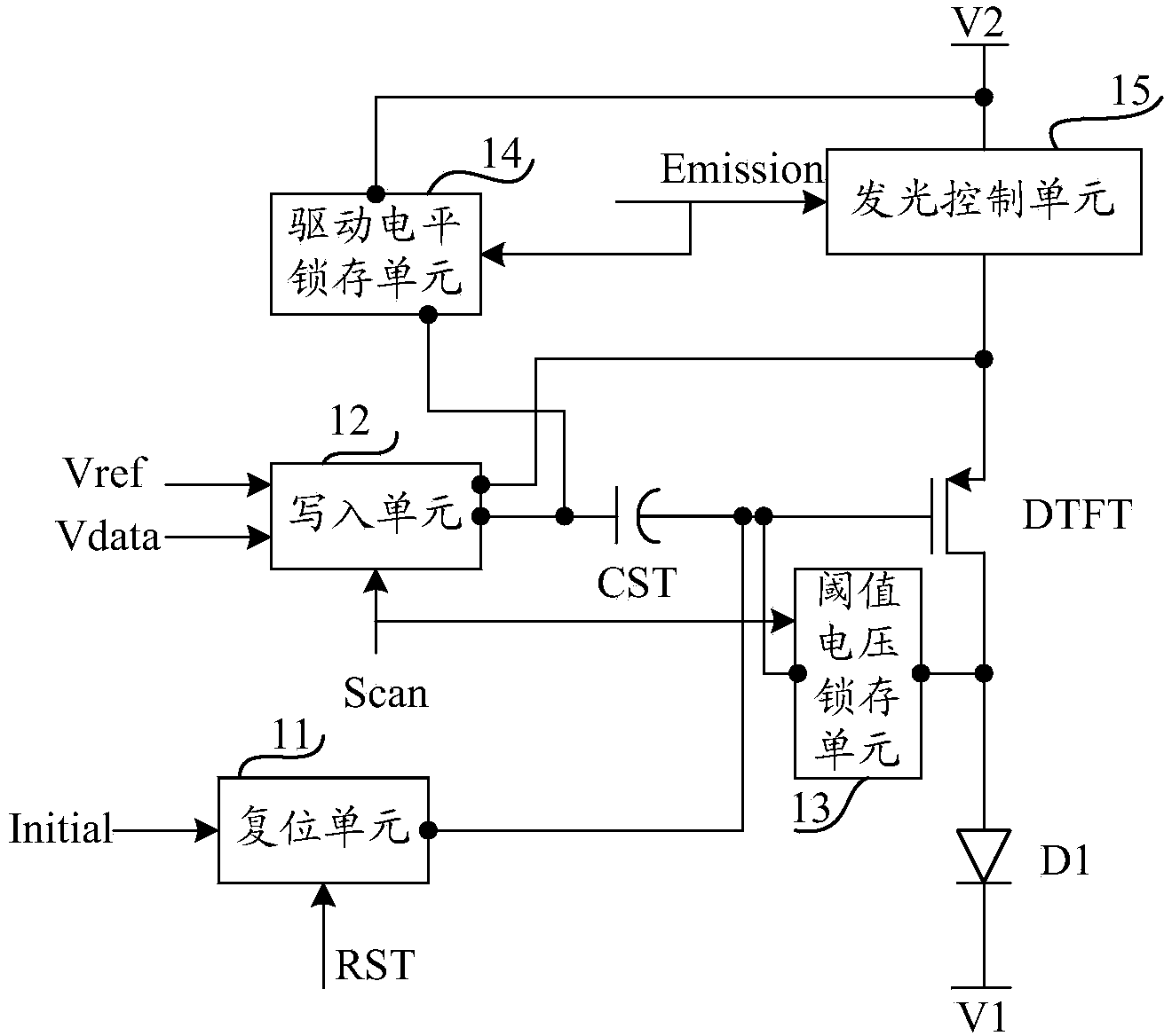
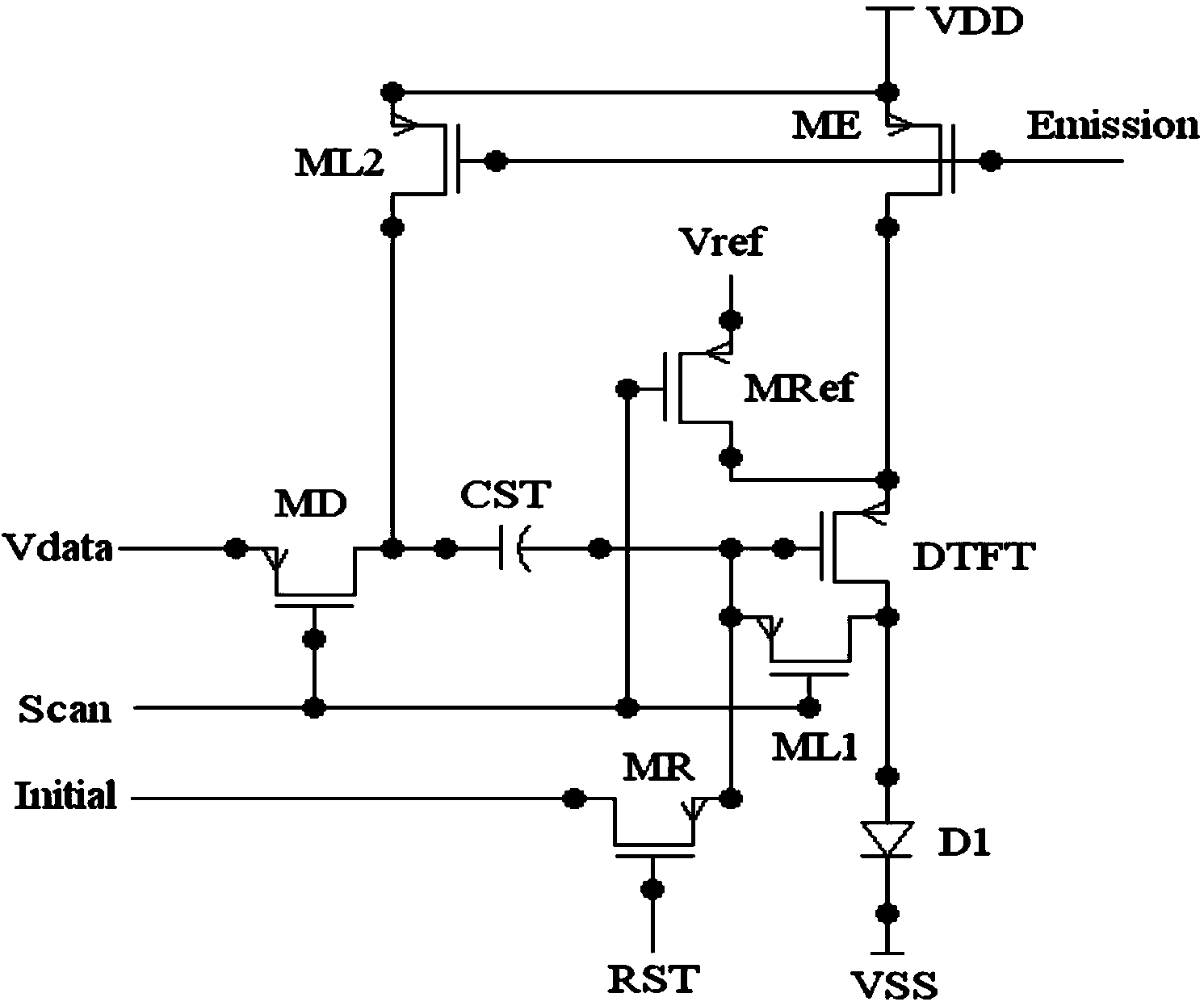
[0031] The pixel circuit described in the embodiment of the present invention includes a driving transistor, a storage capacitor, and a light emitting element; the driving transistor is connected to the first end of the light emitting element, and the second end of the light emitting element is connected to a first driving level ; The first end of the storage capacitor is connected to the gate of the driving transistor; the pixel circuit also includes:

[0032...


PUM


Abstract

The invention provides a pixel circuit, a driving method of the pixel circuit and a display device of the pixel circuit. The pixel circuit comprises a resetting unit, a writing-in unit, a threshold voltage locking unit, a driving electric level locking unit and a light-emitting control unit. The resetting unit can enable resetting voltage to be access to a grid electrode of a driving transistor to reset the driving transistor, the writing-in unit can write data voltage into the second end of a storage capacitor and can write reference voltage into the second pole of the driving transistor, the threshold voltage locking unit can conduct the connection between the grid electrode of the driving transistor and the first pole of the driving transistor to lock the threshold voltage of the driving transistor into the grid electrode of the driving transistor, the driving electric level locking unit can lock the second driving electric level into the second end of the storage capacitor, and the light-emitting control unit can enable the second driving electric level to be access to the second pole of the driving transistor to control the driving transistor to drive light-emitting elements to emit light after the threshold voltage is locked in the grid electrode of the driving transistor. The grid source voltage of the driving transistor can compensate the threshold voltage of the driving transistor and the second driving electric level. The pixel circuit can improve the effect of compensating the driving electric level.

Description

technical field [0001] The present invention relates to the field of display technology, in particular to a pixel circuit, a driving method thereof, and a display device. Background technique [0002] In an existing pixel circuit applied to an AMOLED (Active Matrix / Organic Light Emitting Diode, Active Matrix Organic Light Emitting Diode) display device, the drive level VDD and the threshold voltage Vth of the drive transistor are latched synchronously. In the latch stage, the drive transistor adopts diode connection mode, which is equivalent to charging a super large resistor and capacitor through the source of the drive transistor, so charging the capacitor is very slow, and it cannot be fully charged to the predetermined voltage within a certain period of time. Charging to a certain voltage, the ratio of the voltage to the predetermined voltage is the charging rate, so the latched driving level VDD should be multiplied by the charging rate, so that the driving level VDD ca...

Claims


Application Information

Patent Timeline
Patent Type & Authority Applications(China)
IPC IPC(8): G09G3/32G09G3/3225
CPCG09G3/3233G09G2300/0819G09G2300/0842G09G2300/0861G09G3/3225G09G2310/0243
Inventor 马占洁
Owner BOE TECH GRP CO LTD
Why Eureka
Try Eureka