LED chip encapsulated without routing and encapsulation technology

A technology of LED chips and packaging technology, applied in electrical components, circuits, semiconductor devices, etc., can solve the problems of limiting the packaging cost of LED chips, unable to overcome the decline of light output, etc., to improve the light output and light output efficiency, and improve the quality of products. rate, overcoming the effect of low yield rate

Inactive Publication Date: 2014-10-01
TOPCHIP TECH COMPANY
View PDF5 Cites 2 Cited by
  • Summary
  • Abstract
  • Description
  • Claims
  • Application Information

AI Technical Summary

Problems solved by technology

[0003] When making this kind of LED chip, the substrate 6 used is a conductive semiconductor structure. Although the above-mentioned vertical chip is the most direct and reasonable method, it also limits the subsequent packaging and packaging costs of the LED chip, which is unavoidable. Yield loss and cost increase due to wire bonding, and problems such as decreased light output due to electrode shadowing cannot be overcome

Method used


Image

  • LED chip encapsulated without routing and encapsulation technology
  • LED chip encapsulated without routing and encapsulation technology
  • LED chip encapsulated without routing and encapsulation technology

Examples


Embodiment Construction

[0020] In order to describe the technical content, structural features, achieved goals and effects of the present invention in detail, the following will be described in detail in conjunction with the embodiments and accompanying drawings.

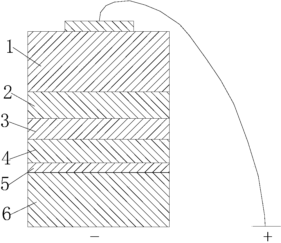
[0021] Compared with the prior art in the present invention, the positive electrode extends upward along the substrate to the transparent conductive layer, the isolation region is arranged between the positive electrode and the negative electrode, and the isolation region is arranged between the positive electrode and the negative electrode And extend upward to the transparent conductive layer. The invention guides the positive and negative poles to the bottom of the LED chip, overcomes the problem of low yield rate caused by strip wires, and improves the yield rate of products.

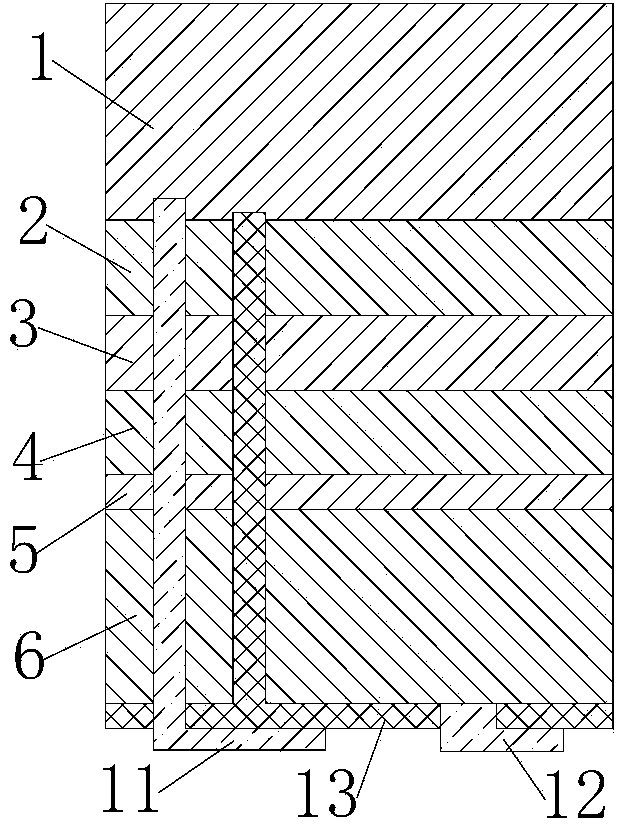
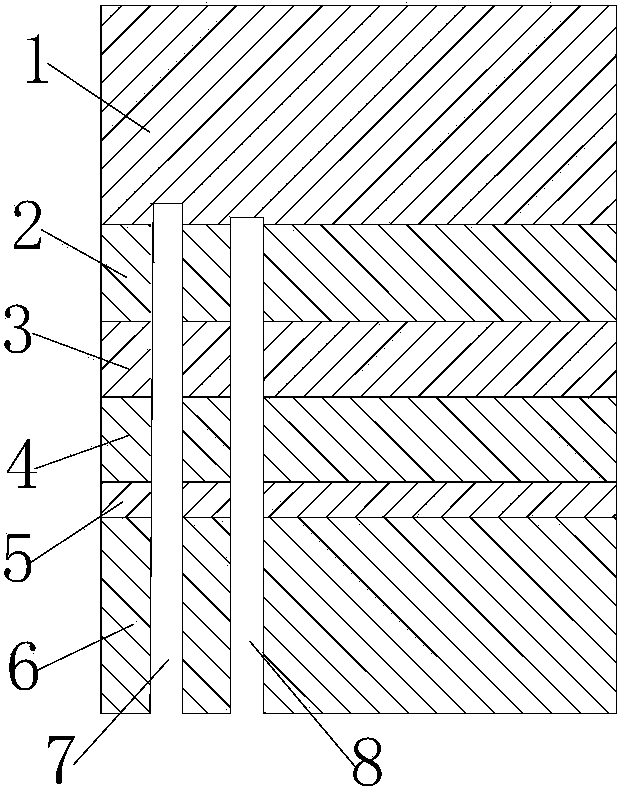
[0022] Such as figure 2 The LED chip in the wire-free packaging shown includes a transparent conductive layer 1, a first light-transmitting layer 2, a light-em...


PUM


Abstract

The invention discloses an LED chip encapsulated without routing. The LED chip encapsulated without routing sequentially comprises a transparent conducting layer, an emitting layer and a liner from the top to the bottom; the LED chip encapsulated without routing further comprises a positive electrode, a negative electrode and an isolation region, wherein the positive electrode extends upwards to the transparent conducting layer along the liner; the isolation region is arranged between the positive electrode and the negative electrode and extends upwards to the transparent conducting layer. The invention further discloses an encapsulation technology. The encapsulation technology comprises the following steps: the negative electrode is arranged on the liner; the positive electrode is arranged on the liner and the positive electrode is enabled to be connected with the transparent conducting layer; an isolation aisle allowing the negative electrode to be isolated from the positive electrode is arranged. The LED chip encapsulated without routing and the encapsulation technology overcome the problem of low qualification rate caused by belt lines; the qualification rate of the product is improved.

Description

technical field [0001] The invention relates to the field of lighting equipment, in particular to a wire-free packaged LED chip and a package process. Background technique [0002] LED chips are the core components of LEDs, etc., and their main function is to convert electrical energy into light energy. At present, the specific structure of traditional LED chips is as follows: figure 1 As shown, it includes a transparent conductive layer 1, a first light-transmitting layer 2, a light-emitting layer 3, a second light-transmitting layer 4, a reflective layer 5, and a substrate 6 from top to bottom. This kind of LED chip is connected to the negative electrode with the substrate, and the positive electrode is connected to the transparent conductive layer by wire bonding. [0003] When making this kind of LED chip, the substrate 6 used is a conductive semiconductor structure. Although the above-mentioned vertical chip is the most direct and reasonable method, it also limits the ...

Claims


Application Information

Patent Timeline
Patent Type & Authority Applications(China)
IPC IPC(8): H01L33/38
CPCH01L33/382H01L2933/0016
Inventor 庞晓东陈浩明王瑞庆刘镇
Owner TOPCHIP TECH COMPANY
Why Eureka
Try Eureka