AMOLED structure and manufacturing method thereof

A manufacturing method and pixel layer technology, applied in the field of OLED, can solve the problems of reducing slope surface and film layer breakage, etc.

Inactive Publication Date: 2014-10-08
EVERDISPLAY OPTRONICS (SHANGHAI) CO LTD
View PDF3 Cites 4 Cited by
  • Summary
  • Abstract
  • Description
  • Claims
  • Application Information

AI Technical Summary

Problems solved by technology

[0004] The purpose of the present invention is to overcome the defects of the prior art, provide an AMOLED structure and a manufacturing method thereof, which can solve the problem of film layer fracture caused by OLED layer climbing, ensure that the thickness of the original pixel layer and space layer remains unchanged, reduce The slope of the slope is small, so as to avoid the breakage of the OLED film layer

Method used


Image

  • AMOLED structure and manufacturing method thereof
  • AMOLED structure and manufacturing method thereof
  • AMOLED structure and manufacturing method thereof

Examples


Embodiment Construction

[0025] The present invention will be further described below in conjunction with the accompanying drawings and specific embodiments.

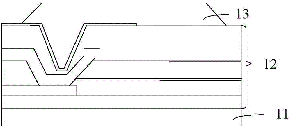
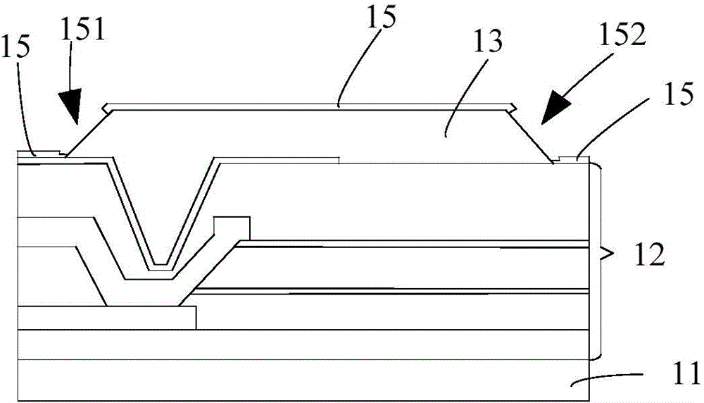
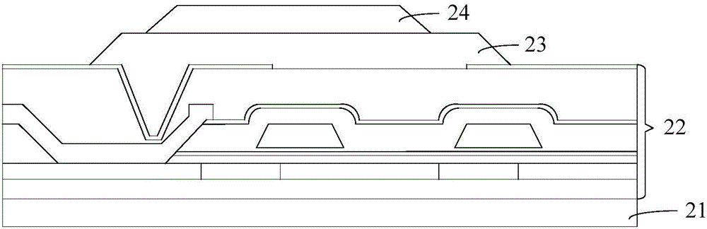
[0026] see Figure 5 As shown, a preferred embodiment of an AMOLED structure of the present invention is shown. The present invention reduces the thickness of the first pixel layer and the second pixel layer by dividing the pixel layer into the first pixel layer and the second pixel layer, thereby reducing the first slope generated on both sides of the first pixel layer and the second pixel layer surface and the slope of the second slope, which is much gentler than the slope of the single-layer pixel layer in the prior art, so in the subsequent OLED film preparation process, there will be no breakage of the OLED film layer, ensuring that the product the quality of. The structure and method for improving the breakage of the OLED film layer of the present invention will be described in detail below in conjunction with the accompanying drawings....


PUM


Abstract

The invention provides an AMOLED structure and a manufacturing method of the AMOLED structure, and the AMOLED structure is used for solving the problem of cracking of an OLED films. The AMOLED structure comprises a TFT circuit layer, a pixel layer on the TFT circuit layer, and an OLED layer on the pixel layer; the pixel layer comprises a first pixel layer and a second pixel layer; the first pixel layer is arranged on the TFT circuit layer, and first slopes are formed on the two sides of the first pixel layer; the second pixel layer is arranged on the first pixel layer, and second slopes are formed on the two sides of the second pixel layer; the OLED layer wraps the TFT circuit layer, the first pixel layer and the second pixel layer. By the adoption of the structure, the problem of cracking of the OLED film can be effectively solved.

Description

technical field [0001] The invention relates to the field of OLEDs, in particular to an AMOLED structure and a manufacturing method for improving the OLED film layer fracture problem. Background technique [0002] Compared with traditional liquid crystal panels, AMOLED (Active Matrix Organic Light Emitting Diode, active matrix organic light emitting diode panel) has the characteristics of fast response speed, high contrast ratio, and wide viewing angle. In addition, AMOLED also has the feature of self-illumination and does not need to use a backlight panel, so it is lighter and thinner than a traditional liquid crystal panel, and can also save the cost of a backlight module. Many advantages make it have a good application prospect. [0003] Existing AMOLEDs have very high requirements in the production process. Generally, the thinner the AMOLED, the better. Therefore, in the AMOLED structure, the OLED layer is made thinner to achieve a light and thin effect. However, consi...

Claims


Application Information

Patent Timeline
IPC IPC(8): H01L51/52H01L51/56
CPCH10K59/122H10K71/00
Inventor 左文霞高印柯其勇
Owner EVERDISPLAY OPTRONICS (SHANGHAI) CO LTD
Why Eureka
Try Eureka