A delay sampling circuit with self-calibration function

A sampling circuit, delay circuit technology, applied in electrical components, electronic switches, pulse technology and other directions, can solve the problems of slow response time, phase deviation, stability and real-time performance of oscillation ring, to prevent measurement deviation, Improve the sampling accuracy, taking into account the effect of real-time and reliability

Active Publication Date: 2017-02-15
SOUTHEAST UNIV
View PDF4 Cites 2 Cited by
  • Summary
  • Abstract
  • Description
  • Claims
  • Application Information

AI Technical Summary

Problems solved by technology

However, the stability of the oscillation ring measurement is poor, and small environmental changes can cause a large phase deviation. This overly sensitive characteristic is not conducive to the monitoring of the chip PVT; in addition, because the cycle measurement of the oscillation ring requires multiple clocks cycles to complete, the response time is relatively slow
For the monitoring unit designed by AVS, the stability and real-time performance of the oscillation ring are not competent
[0008] As a tool for monitoring unit delay, the delay sampling circuit must ensure that PVT changes will not affect the measurement results, which requires the fixed delay area to remain fixed under different PVTs, otherwise the measured replication path delay is inaccurate

Method used


Image

  • A delay sampling circuit with self-calibration function
  • A delay sampling circuit with self-calibration function
  • A delay sampling circuit with self-calibration function

Examples


Embodiment Construction

[0036] The technical solution of the present invention will be described in detail below with a specific design example under the CMOS 0.18 μm process.

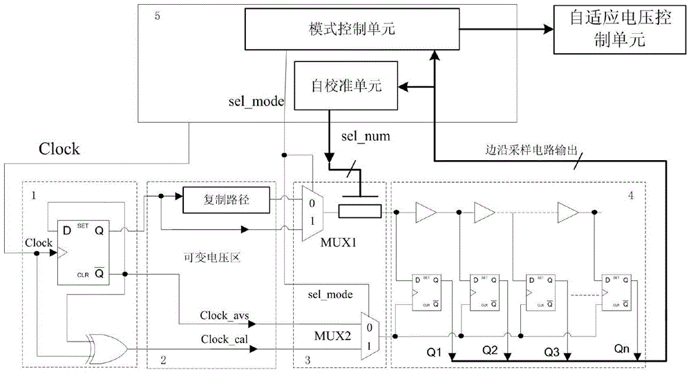
[0037] Such as figure 1 As shown, the delay sampling circuit with self-calibration function of the present invention includes a pulse generation circuit 1, a copy path unit 2, a calibration delay circuit 3, an edge sampling circuit 4 and a delay sampling control module 5, and the calibration delay The circuit 3 includes data selectors MUX1 and MUX2 to select one of the two.

[0038] The pulse generation circuit 1 is composed of a flip-flop and an XOR logic unit. The Q non-output terminal of the flip-flop is connected to the D input terminal, and the output is the frequency division of the reference clock Clock, which is input to the copy path unit 2 as a pulse signal, and the Q non-output The terminal signal is used as the sampling clock Clock_avs in the adaptive adjustment mode, and the Q non-terminal signal is different fr...


PUM


Abstract

The invention discloses a delay sampling circuit having self-calibration function. The delay sampling circuit includes a pulse generation circuit, a replication path unit, a calibration delay circuit, an edge sampling circuit, and a delay sampling control module, wherein, the replication path unit is in a variable voltage area, and other parts are in a fixed voltage area. The invention can be applied to reflect a time sequence condition of a chip and to guide voltage scaling of the chip. Two operation modes of a self-calibration mode and an adaptive voltage scaling mode are provided according to the delay sampling circuit, and cooperate with adaptive voltage scaling to operate together, which can prevent measurement deviation of the chip that results from environment change during operation, thus simultaneously giving consideration to real-time performance and reliability, and can allow the monitored circuit to operate in the required lowest voltage, thus reducing power consumption of the circuit effectively.

Description

technical field [0001] The invention relates to a delay sampling circuit with a self-calibration function, which can be used to reflect the timing deviation of a chip due to changes in technology, temperature and voltage conditions. The whole circuit is realized by pure digital logic, which belongs to the field of digital integrated circuit design. [0002] technical background [0003] With the further shrinking of the IC process size and the rapid development of handheld mobile devices, power consumption has become an important indicator in system chip design. In the traditional digital integrated circuit design process, in order to cope with the circuit changes in the worst case, the designer usually chooses the worst case as the design condition of the chip. fluctuations, process deviations (such as gate length fluctuations, doping fluctuations, etc.), coupling noise and other adverse effects of parameter fluctuations, but these adverse timing deviation factors are actua...

Claims


Application Information

Patent Timeline
Patent Type & Authority Patents(China)
IPC IPC(8): H03K17/28
Inventor 单伟伟金海坤
Owner SOUTHEAST UNIV
Why Eureka
Try Eureka