CMOS image sensor pixel

An image sensor and pixel technology, applied in the field of image sensors, can solve the problems of small illumination range, inability to identify physical information, inability to collect signals, etc., to overcome the small dynamic range and expand the photosensitive dynamic range.

Inactive Publication Date: 2014-11-05
BEIJING SUPERPIX MICRO TECHNOLOGY CO LTD
View PDF6 Cites 5 Cited by
  • Summary
  • Abstract
  • Description
  • Claims
  • Application Information

AI Technical Summary

Problems solved by technology

[0006] The light range detected by the above-mentioned linear sensor is small, especially in a high-light environment, it is impossible to recognize the physical information, and it cannot collect all the signals from the change of the dark light environment to the strong light environment, which is called a small dynamic range in the industry, so Reduced sensor output image quality

Method used


Image

  • CMOS image sensor pixel
  • CMOS image sensor pixel
  • CMOS image sensor pixel

Examples


specific Embodiment

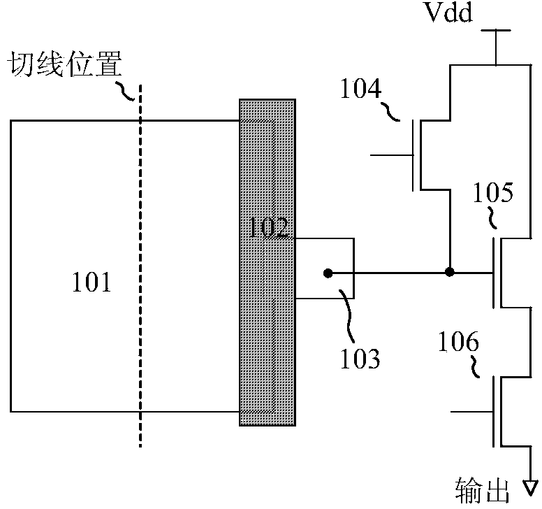
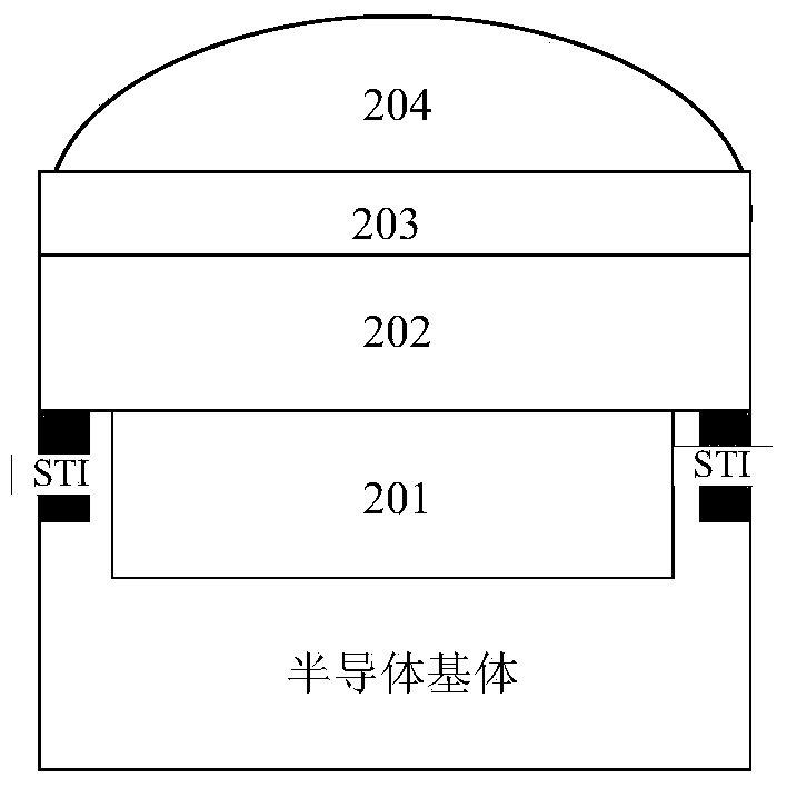
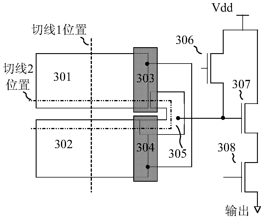
[0030] In order to improve the quality of the output image of the image sensor, the present invention starts from improving the pixel structure of the image sensor in the prior art. Two photodiodes are arranged in the pixel structure of the present invention. The areas of the two photodiodes can be the same or different, and the two Microlenses are respectively arranged above the two photodiodes, and the planar areas of the two microlenses are different, so the amount of light collected is different, and one of the two photodiodes will be saturated before the other. Before one of the photodiodes is saturated, the photosensitive sensitivity of the pixel is higher; after saturation, the saturated photodiode will not continue to collect photoelectric charges, and only the unsaturated photodiode will collect photoelectric charges, so the overall photosensitive sensitivity of the pixel will decrease.

[0031] The following takes the four-transistor pixel structure as an example to e...


PUM


Abstract

The invention discloses a CMOS image sensor pixel which comprises a first photodiode and a second photodiode. The first photodiode and the second photodiode are connected with a first charge transfer transistor and a second charge transfer transistor respectively. The first charge transfer transistor and the second charge transfer transistor share a floating active area. A first micro lens and a second micro lens are arranged above the first charge transfer transistor and the second charge transfer transistor respectively. Color filters are arranged between the portions above the first photodiode and the second photodiode and the portions below the first micro lens and the second micro lens. The luminous sensitivity of the pixel in the floodlighting process is improved, the sensitization dynamic range of the pixel is expanded, the defect that the dynamic range of a linear image sensor is small can be overcome, and more detailed information of an image in a floodlighting environment can be collected.

Description

technical field [0001] The invention relates to an image sensor, in particular to a CMOS image sensor pixel. Background technique [0002] The image sensor uses the photosensitive elements in the photosensitive pixel array to collect image information, converts the pixel image signal into a pixel photoelectric signal, and then restores the real image information of each pixel through image signal processing operations. [0003] For image sensor pixels in the prior art, taking CMOS image sensor pixels as an example, one pixel is only provided with one photosensitive element, such as figure 1 shown; figure 1 Among them, 101 is a photodiode, 102 is a charge transfer transistor, 103 is a floating active region, 104 is a reset transistor, 105 is a source follower transistor, 106 is a selection transistor, and Vdd is a power supply voltage. figure 1 In the pixel structure in , only one photodiode is used, and the sectional structure above the photodiode, such as figure 2 shown...

Claims


Application Information

Patent Timeline
Patent Type & Authority Applications(China)
IPC IPC(8): H04N5/374H01L27/146
Inventor 郭同辉旷章曲
Owner BEIJING SUPERPIX MICRO TECHNOLOGY CO LTD
Why Eureka
Try Eureka