Sensitivity Adaptive Image Sensor Pixel Structure
An image sensor and pixel structure technology, applied in the field of image sensors, can solve the problems of poor image acquisition ability, high sensitivity, and low sensitivity, and achieve the effect of expanding the dynamic range of photosensitivity, high sensitivity, and compressing photosensitivity
- Summary
- Abstract
- Description
- Claims
- Application Information
AI Technical Summary
Problems solved by technology
Method used
Image
Examples
specific Embodiment
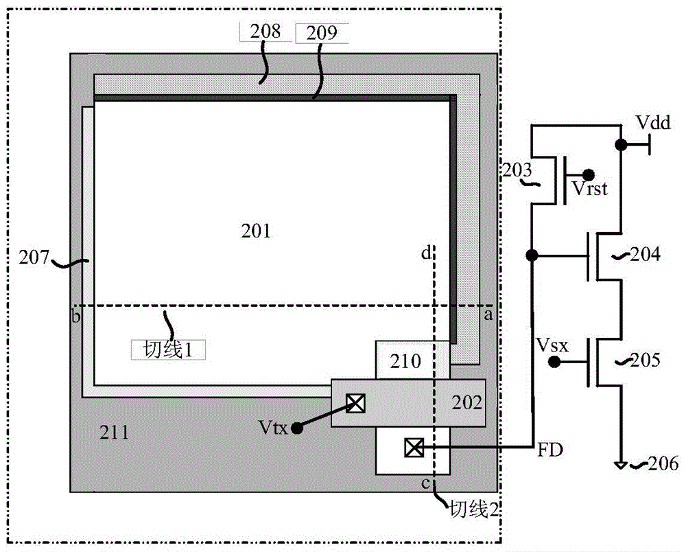
[0038] Image sensor pixel structure such as figure 2 As shown, it includes the planar part inside the dotted line box and the schematic diagram of the circuit part outside the dotted line box. figure 2 Among them, 201 is a photodiode area, 202 is a charge transfer transistor, 203 is a reset transistor, FD is a floating active area, 204 is a source follower transistor, 205 is a selection transistor, 206 is a signal output terminal, and 207 is a P-type ion isolation area , 208 is the gate polysilicon of the transistor capacitor device, 209 is the thin oxide layer of the transistor capacitor device, 210 is the charge storage area, 211 is the shallow trench isolation area;
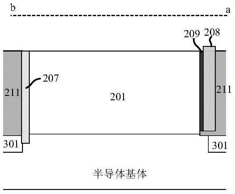
[0039] Where Vtx is the gate terminal of the charge transfer transistor 202, Vrst is the gate terminal of the reset transistor 203, Vsx is the gate terminal of the selection transistor 205, FD is the floating active region, Vdd is the power supply voltage, and tangents 1 and 2 indicate positions respectively...
PUM
 Abstract
Description
Claims
Application Information


