Unlock instant, AI-driven research and patent intelligence for your innovation.

A kind of thin film transistor and its preparation method, array substrate, liquid crystal display device

A thin-film transistor and thin-film technology, applied in the direction of transistors, semiconductor/solid-state device manufacturing, electric solid-state devices, etc., to achieve the effects of avoiding hole leakage current, simple preparation process, and avoiding photo-induced leakage current

Active Publication Date: 2017-02-15
BOE TECH GRP CO LTD +1
View PDF6 Cites 0 Cited by
  • Summary
  • Abstract
  • Description
  • Claims
  • Application Information

AI Technical Summary

Problems solved by technology

[0005] However, in the actual process often appear as figure 2 and image 3 the situation shown
in, figure 2 Shown is the case where the size of the gate 101 is smaller than that of the amorphous silicon layer 103. Since the gate 101 cannot completely cover the amorphous silicon layer 103, the light from the bottom backlight will hit the amorphous silicon layer 103, resulting in photoleakage. electric current

Method used


Image

  • A kind of thin film transistor and its preparation method, array substrate, liquid crystal display device
  • A kind of thin film transistor and its preparation method, array substrate, liquid crystal display device
  • A kind of thin film transistor and its preparation method, array substrate, liquid crystal display device

Examples


Embodiment Construction

[0034] The following will clearly and completely describe the technical solutions in the embodiments of the present invention with reference to the accompanying drawings in the embodiments of the present invention. Obviously, the described embodiments are only some, not all, embodiments of the present invention. Based on the embodiments of the present invention, all other embodiments obtained by persons of ordinary skill in the art without making creative efforts belong to the protection scope of the present invention.

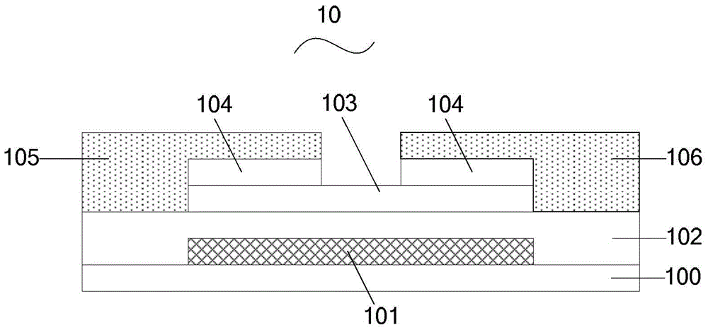
[0035] An embodiment of the present invention provides a thin film transistor 10, such as Figure 4 and Figure 5As shown, the thin film transistor 10 includes: a gate 101, an amorphous silicon layer 103 and an ohmic contact layer 104 sequentially arranged on a base substrate 100, the size of the gate 101 is smaller than the size of the amorphous silicon layer 103 ; On this basis, the thin film transistor 10 also includes: a light blocking layer 107 arranged ...


PUM


Abstract

The invention provides a thin film transistor and a preparation method thereof, as well as an array baseplate and a liquid crystal display device, relates to the technical field of display, can enable a preparation technology of the thin film transistor to be simpler, and can avoid generating photoinduced leakage current and hole leakage current. The thin film transistor comprises a gate electrode, an amorphous silicon layer and an ohmic contact layer which are arranged on an underlay baseplate in sequence; the size of the gate electrode is smaller than that of the amorphous silicon layer; on the basis, the thin film transistor further comprises a light blocking layer which is arranged between the amorphous silicon layer and the underlay baseplate, corresponding to the rest part, not being blocked by the gate electrode, of the amorphous silicon layer, and beyond the amorphous silicon layer. The invention is used for designing and manufacturing the thin film transistor, the array baseplate comprising the thin film transistor, and the liquid crystal display device comprising the array baseplate.

Description

technical field [0001] The invention relates to the field of display technology, in particular to a thin film transistor, a preparation method, an array substrate, and a liquid crystal display device. Background technique [0002] In a liquid crystal display device, the leakage current of a thin film transistor (TFT for short) will seriously affect the characteristics of the thin film transistor. Therefore, how to reduce the leakage current of the thin film transistor has always been a subject of research by those skilled in the art. [0003] Such as figure 1 , 2 , 3, the thin film transistor 10 may include a gate 101, a gate insulating layer 102, an amorphous silicon layer 103, an ohmic contact layer 104 (n+ amorphous silicon layer), and a source 105 and drain 106 . [0004] The ideal thin film transistor 10 has a structure such as figure 1 As shown, wherein the size of the gate 101 is consistent with that of the amorphous silicon layer 103 . In this way, on the one ha...

Claims


Application Information

Patent Timeline
Patent Type & Authority Patents(China)
IPC IPC(8): H01L29/786H01L29/423H01L23/552H01L21/336
Inventor 肖昂
Owner BOE TECH GRP CO LTD