
Data reading method, control circuit, memory module, and memory device of memory

A technology for reading memory modules and data, applied in the direction of read-only memory, static memory, information storage, etc., can solve the problem that the flash memory element 1 cannot be correctly identified in the storage state, the electronic writing speed is increased, and the flash memory element 1 wear and tear and other issues

Active Publication Date: 2014-11-26
PHISON ELECTRONICS
View PDF4 Cites 8 Cited by
  • Summary
  • Abstract
  • Description
  • Claims
  • Application Information

AI Technical Summary

Problems solved by technology

[0005] During the writing and erasing process, the flash memory device 1 will wear out due to the repeated injection and removal of electrons, which will increase the writing speed of electrons and cause the threshold voltage distribution to widen
Therefore, after multiple times of writing and erasing, the flash memory device 1 may not be able to correctly identify its storage state, resulting in erroneous bits.

Method used


Image

  • Data reading method, control circuit, memory module, and memory device of memory
  • Data reading method, control circuit, memory module, and memory device of memory
  • Data reading method, control circuit, memory module, and memory device of memory

Examples


Embodiment Construction

[0119] Generally speaking, a memory storage device (also called a memory storage system) includes a rewritable non-volatile memory module and a controller (also called a control circuit). Typically memory storage devices are used with a host system such that the host system can write data to or read data from the memory storage device.

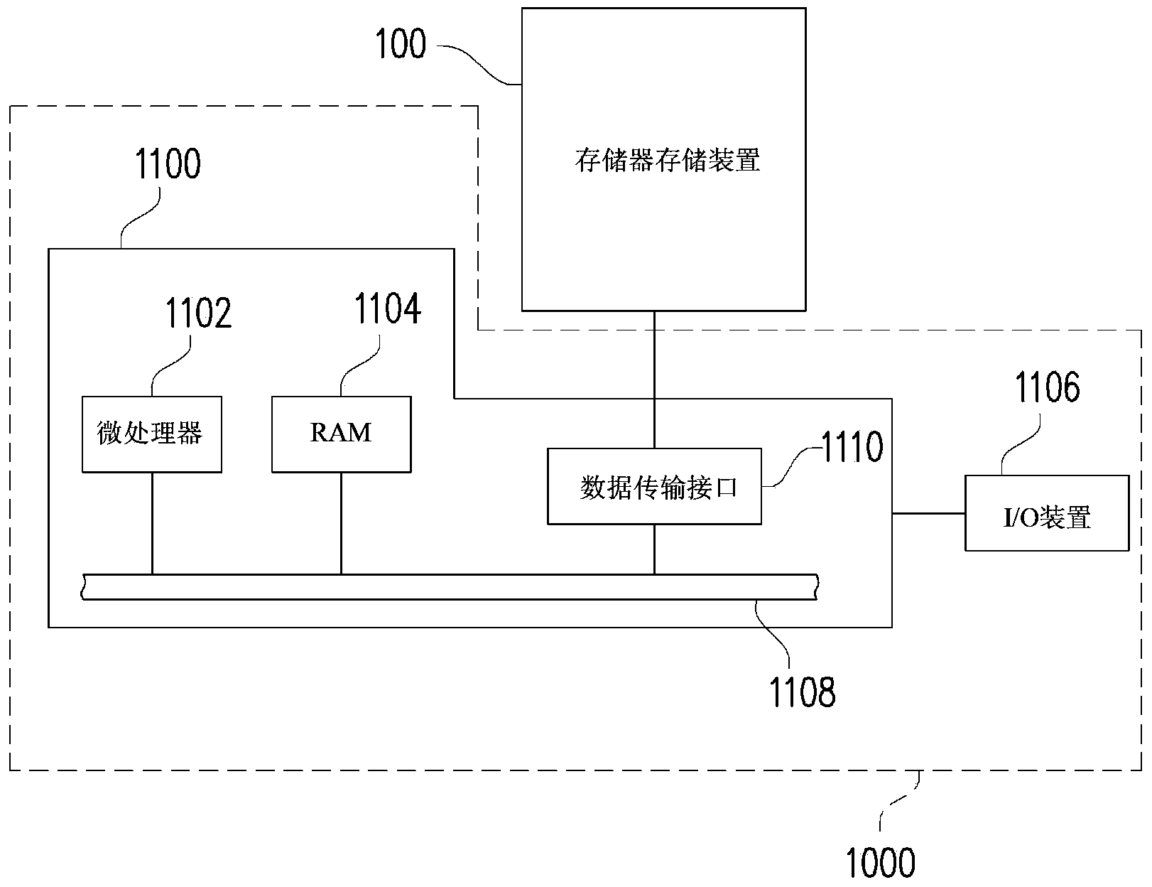
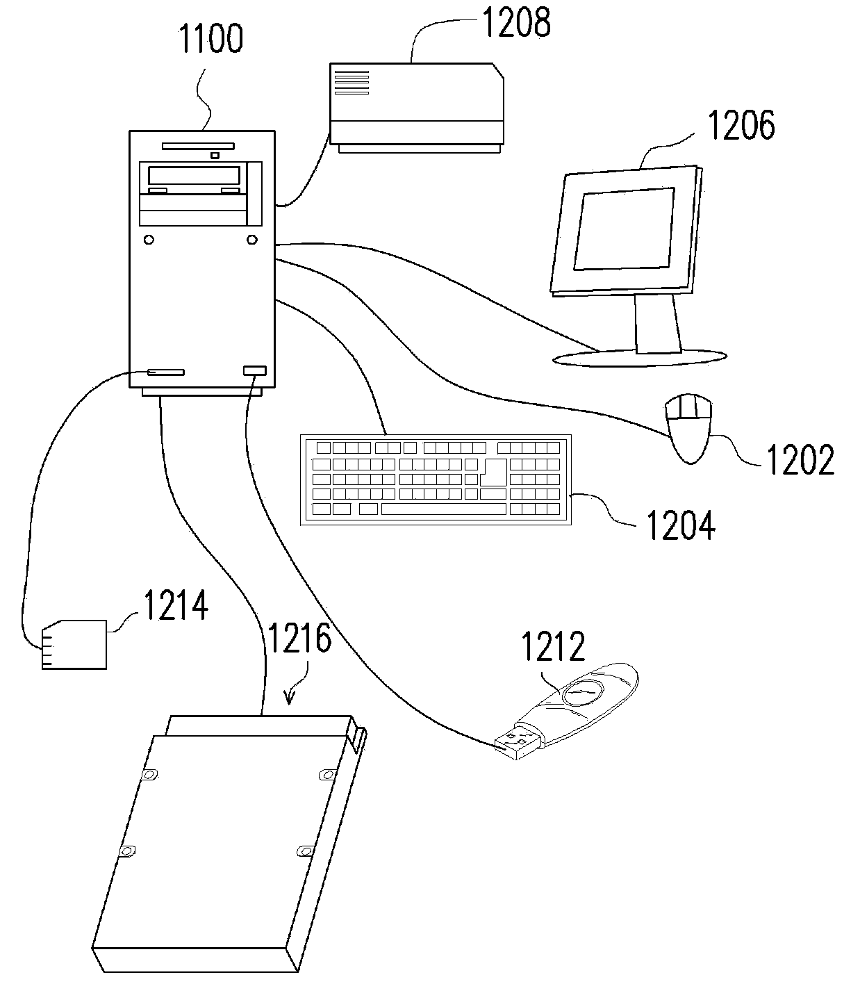
[0120] figure 2 is a schematic diagram of a host system and a memory storage device shown according to an embodiment, image 3 is a schematic diagram of a computer, an input / output device and a memory storage device according to an embodiment, Figure 4 It is a schematic diagram of a host system and a memory storage device according to an embodiment.

[0121] Please refer to figure 2 , the host system 1000 generally includes a computer 1100 and an input / output (I / O) device 1106 . The computer 1100 includes a microprocessor 1102 , a random access memory (random access memory, RAM) 1104 , a system bus 1108 and a data transmission interface...


PUM


Abstract

The invention provides a data reading method, a control circuit, a memory module, and a memory device of memory, wherein the data reading method, the control circuit, the memory module, and the memory device of memory can be applied to a rewritable nonvolatile memory module. The method comprises a step of determining a corresponding read voltage according to the critical voltage distribution of a memory element of a word line. The method also comprises the following steps: if the critical voltage distributions of a plurality of memory elements are all right deviation distribution, applying right adjusting voltage group of the read voltage to the word line to read a plurality of bit data as the corresponding soft values; and obtaining the page data in the plurality of memory elements through the soft values corresponding to coding; wherein the right adjusting voltage group comprises a plurality of positive adjusting read voltage and a plurality of negative adjusting read voltage, and the number of the positive adjusting read voltage is more than that of the negative adjusting read voltage. Through the technical scheme mentioned above, the method can correctly recognize the storage state of the memory elements.

Description

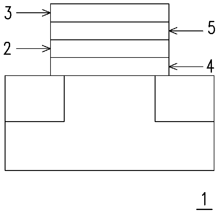
technical field [0001] The invention relates to a data reading method, a control circuit, a memory module and a memory storage device. Background technique [0002] Digital cameras, mobile phones, and MP3 players have grown rapidly in recent years, making consumers' demand for storage media also increase rapidly. Because rewritable non-volatile memory (rewritable non-volatile memory) has the characteristics of data non-volatility, power saving, small size, no mechanical structure, fast read and write speed, etc., it is most suitable for portable electronic products, such as laptop. A solid state drive is a storage device that uses flash memory as a storage medium. Therefore, the flash memory industry has become a very popular part of the electronics industry in recent years. [0003] figure 1 is a schematic diagram of a flash memory element shown according to the prior art. [0004] Please refer to figure 1 , the flash memory element 1 includes a charge trapping layer ...

Claims


Application Information

Patent Timeline
IPC IPC(8): G11C16/06G11C16/26
Inventor 郑国义林纬林玉祥严绍维赖国欣
Owner PHISON ELECTRONICS
Learn More