Measuring circuit for breakover voltage drop of semiconductor switch device

A switching device and conduction voltage drop technology, which is applied in the direction of single semiconductor device testing, circuit breaker testing, etc., can solve the problems of slow response speed, poor anti-interference ability, and low accuracy, so as to improve the measurement accuracy and reduce the Effects of improving dynamic range and safety

Active Publication Date: 2014-12-03
SHANGHAI UNITED IMAGING HEALTHCARE
View PDF4 Cites 22 Cited by
  • Summary
  • Abstract
  • Description
  • Claims
  • Application Information

AI Technical Summary

Problems solved by technology

[0009] In view of the shortcomings of the prior art described above, the purpose of the present invention is to provide a measurement circuit for the conduction voltage drop of a semiconductor switching device, which is used to solve the problem of low accuracy of the measurement circuit for the conduction voltage drop of a semiconductor switching device in the prior art, Problems such as slow response speed, complex circuit, poor anti-interference ability, and large dynamic range of the signal to be tested

Method used


Image

  • Measuring circuit for breakover voltage drop of semiconductor switch device
  • Measuring circuit for breakover voltage drop of semiconductor switch device
  • Measuring circuit for breakover voltage drop of semiconductor switch device

Examples


Embodiment Construction

[0077] Embodiments of the present invention are described below through specific examples, and those skilled in the art can easily understand other advantages and effects of the present invention from the content disclosed in this specification. The present invention can also be implemented or applied through other different specific implementation modes, and various modifications or changes can be made to the details in this specification based on different viewpoints and applications without departing from the spirit of the present invention.

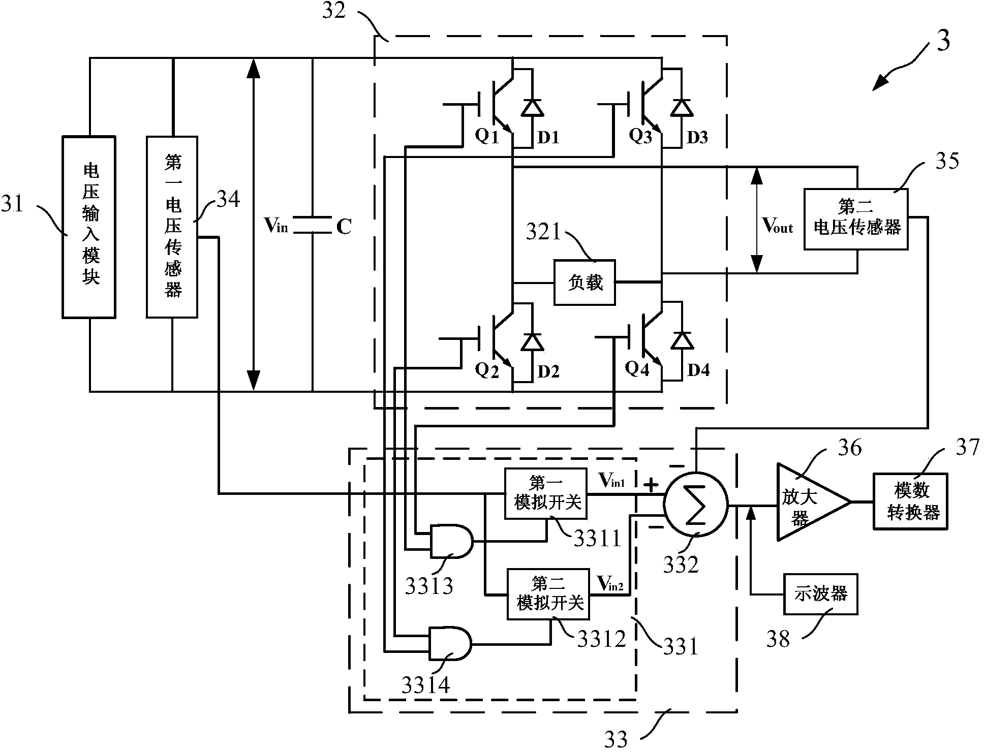
[0078] see Figure 3 ~ Figure 11 . It should be noted that the diagrams provided in this embodiment are only schematically illustrating the basic idea of ​​the present invention, and only the components related to the present invention are shown in the diagrams rather than the number, shape and shape of the components in actual implementation. Dimensional drawing, the type, quantity and proportion of each component can be changed arb...


PUM


Abstract

The invention provides a measuring circuit for a breakover voltage drop of a semiconductor switch device. The measuring circuit comprises a voltage input module, an inversion module and a testing module, wherein the voltage input module is used for providing input voltage, the inversion module is connected to the voltage input module in parallel, and the testing module is used for sampling the input voltage to obtain sampling voltage and carrying out the subtraction operation on the sampling voltage and output voltage of the inversion module to obtain the breakover voltage drop of the semiconductor switch device in the inversion module. The invention relates to a real-time on-line testing method, and changes of the breakover voltage drop caused by changes of junction temperature and collector electrode currents can be reflected more accurately in time; electric isolation is achieved based on the Hall effect, so that safety of the circuit is greatly improved; in addition, the circuit is simple in structure, the breakover voltage of the semiconductor switch device is calculated by measuring the difference of the direct-current bus voltage and the output voltage, the dynamic range of signals to be detected is greatly narrowed, and therefore the measurement accuracy is improved.

Description

technical field [0001] The invention relates to the field of power electronic control, in particular to a measurement circuit for conducting voltage drop of a semiconductor switching device. Background technique [0002] Semiconductor switching devices are small in size, light in weight, low in power consumption, long in life, and high in reliability. They are widely used in power supplies, motor control, inverters, and other fields. Their performance determines the quality of the product. The conduction voltage drop is one of the important parameters of the semiconductor switching device, which is directly related to the output power and output current capability of the device. The smaller the conduction voltage drop of the semiconductor switching device, the greater the on-state current it can withstand. In addition, the conduction voltage drop of the semiconductor switching device is also related to the temperature rise of the device and its own power consumption. The lar...

Claims


Application Information

Patent Timeline
Patent Type & Authority Applications(China)
IPC IPC(8): G01R31/327G01R31/26
Inventor 刘慧芳褚旭罗颖鹏
Owner SHANGHAI UNITED IMAGING HEALTHCARE
Why Eureka
Try Eureka