Fingerprint identification sensor packaging structure and method

A fingerprint identification and packaging structure technology, which is applied in character and pattern recognition, instruments, electric solid devices, etc., can solve the problem of low recognition accuracy of capacitive fingerprint recognition sensors and ineffective capacitive sensing effects of capacitive fingerprint recognition sensors, etc. problem, to achieve the effect of improving recognition accuracy, increasing recognition distance, and sensing

Active Publication Date: 2014-12-03
NANCHANG OUFEI BIOLOGICAL IDENTIFICATION TECH
View PDF3 Cites 9 Cited by
  • Summary
  • Abstract
  • Description
  • Claims
  • Application Information

AI Technical Summary

Problems solved by technology

[0004] However, due to the existing capacitive fingerprint recognition sensor packaging structure, the fingerprint recognition sensor is placed under the control button or display element where the capacitive sensing is not obvious, so that the capacitance sensing effect of the capacitive fingerprint recognition sensor is not obvious, resulting in the capacitive fingerprint recognition. The recognition accuracy of the sensor is not high

Method used


Image

  • Fingerprint identification sensor packaging structure and method
  • Fingerprint identification sensor packaging structure and method
  • Fingerprint identification sensor packaging structure and method

Examples


Embodiment Construction

[0031] In order to make the purpose, technical solutions and advantages of the embodiments of the present invention clearer, the technical solutions in the embodiments of the present invention will be clearly and completely described below in conjunction with the drawings in the embodiments of the present invention. Obviously, the described embodiments It is a part of embodiments of the present invention, but not all embodiments. Based on the embodiments of the present invention, all other embodiments obtained by persons of ordinary skill in the art without creative efforts fall within the protection scope of the present invention.

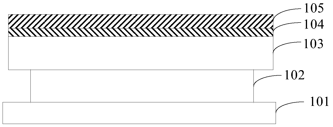
[0032] figure 1 It is a schematic cross-sectional view of the packaging structure of the fingerprint recognition sensor of the present invention Figure 1 . The fingerprint recognition sensor provided in this embodiment can specifically be a capacitive fingerprint recognition sensor, and can be used in electronic devices, such as smart phones, t...


PUM


Abstract

The embodiment of the invention provides a fingerprint identification sensor packaging structure and method. The packaging structure comprises a fingerprint identification sensor arranged above a silicon wafer and electrically connected with the silicon wafer, a color film layer arranged above the fingerprint identification sensor, a hard mask layer arranged above the color film layer and a substrate arranged below the silicon wafer, wherein at least one of the hard mask layer and the color film layer is doped with high dielectric particles. The packaging structure can improve identification accuracy of the fingerprint identification sensor.

Description

technical field [0001] The embodiment of the present invention relates to a biometric identification module packaging technology, in particular to a fingerprint identification sensor packaging structure and packaging method. Background technique [0002] With the development of science and technology, electronic sensing technology is being applied more and more. At present, the fingerprint identification (finger printing) technology implemented by electronic sensing technology is the most mature and cheap biometric identification technology, which can be applied to notebook computers, mobile phones, automobiles, banks and other fields. [0003] In the prior art, the fingerprint recognition sensor realized by the biometric identification technology is mainly a matrix-type capacitive fingerprint recognition sensor formed by a Complementary Metal Oxide Semiconductor (CMOS) process. [0004] However, due to the existing capacitive fingerprint recognition sensor packaging struct...

Claims


Application Information

Patent Timeline
Patent Type & Authority Applications(China)
IPC IPC(8): G06K9/00H01L23/31H01L21/56
CPCH01L2224/16225
Inventor 刘伟唐根初蒋芳
Owner NANCHANG OUFEI BIOLOGICAL IDENTIFICATION TECH
Why Eureka
Try Eureka