Solar cell of perovskite structure and preparing method of solar cell
A perovskite structure and solar cell technology, applied in circuits, photovoltaic power generation, electrical components, etc., can solve problems such as single protection, achieve the effects of isolating moisture, improving stability, and improving photovoltaic characteristics
- Summary
- Abstract
- Description
- Claims
- Application Information
AI Technical Summary
Problems solved by technology
Method used
Image
Examples
Embodiment 1
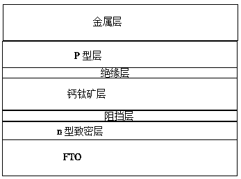
[0061] 1. Select FTO glass with a sheet resistance of 15Ω, a thickness of 2.2mm, and a transmittance of 83% as the substrate material, and then clean it with soap, acetone and ethanol.
[0062] 2. Dense TiO 2 layer preparation
[0063] Same as step 2 in Comparative Example 1.
[0064] 3. Barrier layer Al 2 o 3 Film preparation
[0065] Same as step 3 in Comparative Example 2.
[0066] 4. CH 3 NH 3 PB 3 Preparation of perovskite layer
[0067] Same as step 3 in Comparative Example 1.
[0068] 5. Al insulation layer 2 o 3 Film preparation
[0069] Growth of 3 nm-thick dense Al on perovskite films using ozone and trimethylaluminum as sources 2 o 3 The growth process is as follows: chamber reaction temperature 70°C, trimethylaluminum source for 500ms, nitrogen purge for 20s, ozone for 500ms, nitrogen purge for 20s, repeat the above process 40 times.
[0070] 6. Preparation of hole-conducting layer
[0071] Same as Step 4 in Comparative Example 1.
[0072] 7. Prepa...
Embodiment 2
[0076] 1. Select FTO glass with a sheet resistance of 15Ω, a thickness of 2.2mm, and a transmittance of 83% as the substrate material, and then clean it with soap, acetone and ethanol.
[0077] 2. Preparation of dense ZnO layer
[0078] Use ALD technology to grow a 10nm thick ZnO layer, the deposition conditions: the reaction temperature is 200 ° C, and Zn (CH 2 CH 3 ) 2 1s, nitrogen purge for 1.5s, water flow for 500ms, nitrogen purge for 1s, repeat the above process 100 times.
[0079] 3. Barrier layer Al 2 o 3 Film preparation
[0080] Same as step 3 in Comparative Example 2.
[0081] 4. CH 3 NH 3 PB 3 Preparation of perovskite layer
[0082] Same as step 3 in Comparative Example 1.
[0083] 5. Al insulation layer 2 o 3 Film preparation
[0084] Same as step 5 in Example 1.
[0085] 6. Preparation of hole-conducting layer
[0086] Same as Step 4 in Comparative Example 1.
[0087] 7. Preparation of photocathode
[0088] Same as Step 5 in Comparative Exampl...
PUM
| Property | Measurement | Unit |
|---|---|---|
| thickness | aaaaa | aaaaa |
| thickness | aaaaa | aaaaa |
| thickness | aaaaa | aaaaa |
Abstract
Description
Claims
Application Information


