Memory module and processing module

A memory module and processing module technology, applied in the direction of electric solid-state devices, semiconductor devices, semiconductor/solid-state device components, etc., can solve the problems of labor costs and waste of resources, achieve dynamic memory configuration, realize memory configuration, save manpower and Effect of hardware cost

Inactive Publication Date: 2014-12-10
DAWNING INFORMATION IND BEIJING
View PDF2 Cites 2 Cited by
  • Summary
  • Abstract
  • Description
  • Claims
  • Application Information

AI Technical Summary

Problems solved by technology

[0003] According to different application scenarios, the requirements for each storage resource are also diversified. In the existing technology, since the interface definitions of various storage chips are different, whether ASIC is used as the main chip for network processing or FPGA is used as the main chip for network processing , all customize different hardware boards according to different application scenarios, and weld the memory chips that need to be used on the customized boards, which causes a lot of labor costs and waste of resources

Method used


Image

  • Memory module and processing module

Examples


Embodiment Construction

[0021] The following will clearly and completely describe the technical solutions in the embodiments of the present invention with reference to the accompanying drawings in the embodiments of the present invention. Obviously, the described embodiments are only some, not all, embodiments of the present invention. All other embodiments obtained by persons of ordinary skill in the art based on the embodiments of the present invention belong to the protection scope of the present invention.

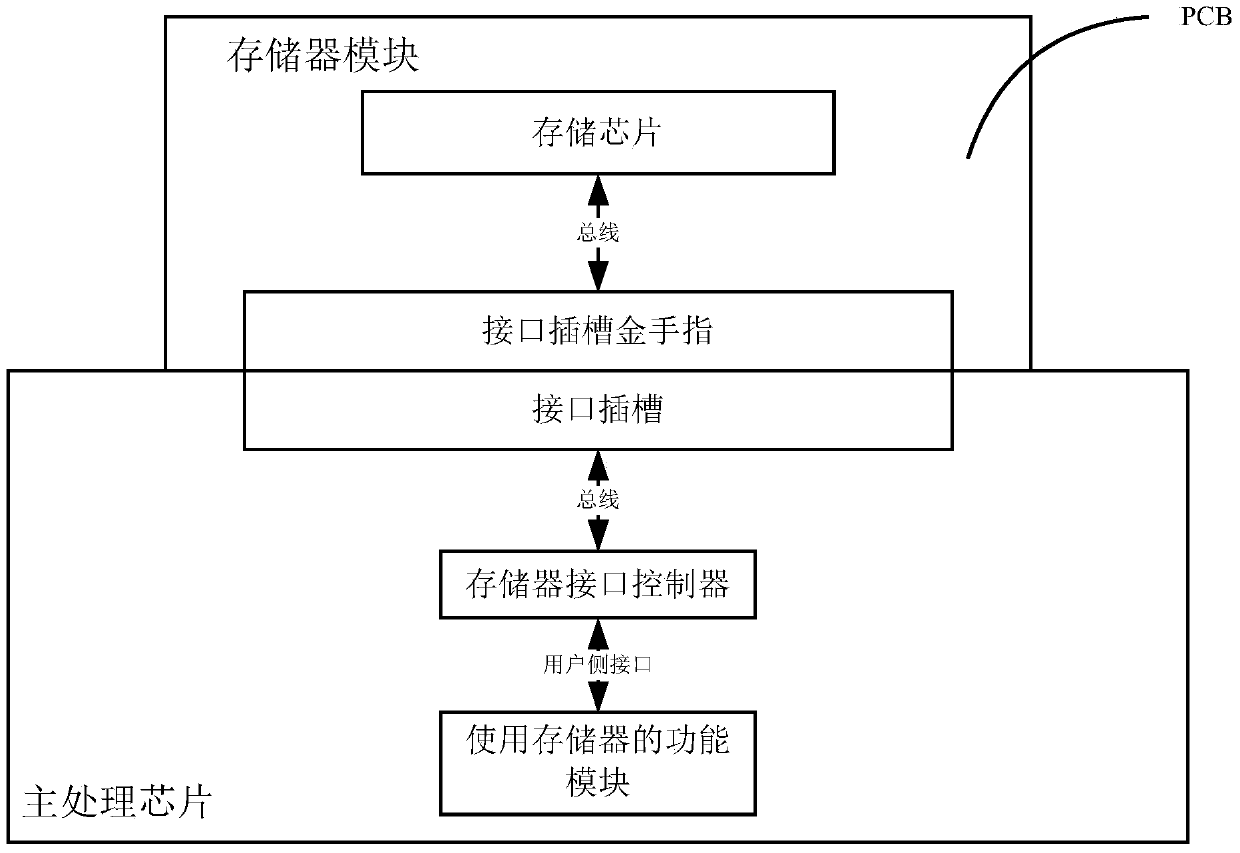
[0022] According to an embodiment of the present invention, a memory module is provided, which can realize the unification of memory chip interfaces, so that it is not necessary to customize different hardware boards for different memory chip types. Such as figure 1 A schematic structural diagram of a memory module and a processing module using the memory module according to an embodiment of the present invention is shown. The memory module includes:

[0023] A printed circuit board (PCB) a...


PUM


Abstract

The invention discloses a memory module and a processing module. The memory module comprises a printed circuit board PCB and at least one memory chip, wherein an interface slot golden finger, a bonding pad of the memory chip, and a bus are comprised on the printed circuit board PCB; the bonding pad is connected with the interface slot golden finger through the bus, the memory chip is welded on the bonding pad to form the memory module. According to the memory module disclosed by the invention, the interfaces of the memory chips are unified, thus customization for different hardware board cards when different types of memory chips needs to be replaced can be avoided, labour and hardware costs are greatly saved, and moreover, dynamic memory configuration can be realized.

Description

technical field [0001] The invention relates to the field of data storage, in particular to a memory module and a processing module. Background technique [0002] In computer network traffic processing equipment such as switches, routers, and firewalls, DRAM, SRAM, and RLDRAM are commonly used memory chips. The places where memory is needed in network traffic processing equipment include: message content storage and routing (switching, ACL ) table storage. Among them, message storage requires large capacity and high bandwidth, and it is more suitable to use DRAM; because the routing (switching, ACL) table is randomly accessed, it has high requirements for low latency, and the requirements for storage capacity vary. When the storage capacity SRAM can be used when the requirements are small, and RLDRAM can be used when the storage capacity requirements are large. [0003] According to different application scenarios, the requirements for each storage resource are also divers...

Claims


Application Information

Patent Timeline
Patent Type & Authority Applications(China)
IPC IPC(8): H01L23/498H01L25/065
Inventor 窦晓光刘新春姚文浩王晖
Owner DAWNING INFORMATION IND BEIJING
Why Eureka
Try Eureka