SRAM unit

A transfer transistor and electrical connection technology, applied in the field of SRAM cells, can solve problems such as the inability to meet the requirements of higher read and write frequencies of SRAM

Active Publication Date: 2014-12-17
SEMICON MFG INT (SHANGHAI) CORP
View PDF1 Cites 6 Cited by
  • Summary
  • Abstract
  • Description
  • Claims
  • Application Information

AI Technical Summary

Problems solved by technology

[0008] The problem solved by the present invention is that, with the continuous increase of the amount of data information in modern society, the existing 6TSRAM unit can no longer meet the requirements for higher read and write frequency of SRAM

Method used


Image

  • SRAM unit
  • SRAM unit
  • SRAM unit

Examples


Embodiment Construction

[0032] The inventor obtains a new SRAM unit through creative work, and the SRAM unit includes 10 transistors (10T), which is a Tripartite Port SRAM (Tripartite Port SRAM) unit.

[0033] In order to make the above objects, features and advantages of the present invention more comprehensible, specific embodiments of the present invention will be described in detail below in conjunction with the accompanying drawings.

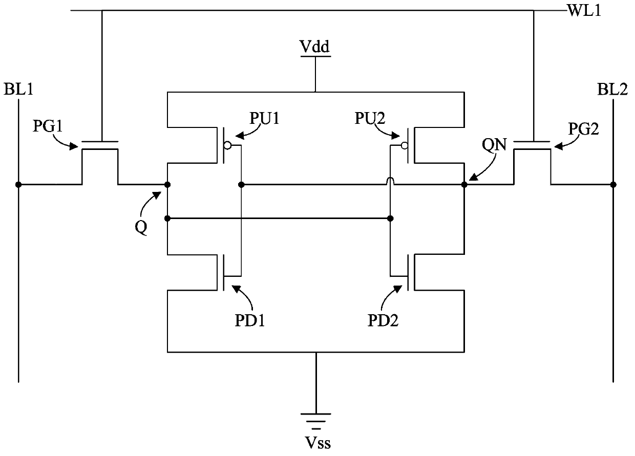
[0034] refer to image 3 , image 3 It is a schematic diagram of the circuit structure of a 10T SRAM unit, the 10T SRAM unit includes: a first inverter 10; a second inverter 20, and the second inverter 20 is cross-coupled with the first inverter 10 to form a latch The first storage node Q and the second storage node QN of information logical value, the first storage node Q and the second storage node QN form a complementary pair; the first pass transistor PG1 and the second pass transistor PG2, the PG1 of the first pass transistor The gate of the second transfer...


PUM


Abstract

The invention relates to an SRAM (static random access memory) unit, which includes a first inverter and a second inverter that are cross coupled to form a first storage node and a second storage node. The grids of a first transmission transistor and a second transmission transistor are electrically connected to a first word line, the grids of a third transmission transistor and a fourth transmission transistor are electrically connected to a second word line, and the grids of a fifth transmission transistor and a sixth transmission transistor are electrically connected to a third word line. The sources of the first transmission transistor and the second transmission transistor are electrically connected to a first bit line and a second bit line respectively, the sources of the third transmission transistor and the fourth transmission transistor are electrically connected to a third bit line and a fourth bit line respectively, and the sources of the fifth transmission transistor and the sixth transmission transistor are electrically connected to a fifth bit line and a sixth bit line respectively. The drain electrodes of the first transmission transistor, the third transmission transistor and the fifth transmission transistor are in electric connection with the first storage node, and the drain electrodes of the second transmission transistor, the fourth transmission transistor and the sixth transmission transistor are in electric connection with the second storage node. Thus, the read-write speed of SRAM can be greatly improved.

Description

technical field [0001] The invention relates to the technical field of semiconductors, in particular to an SRAM unit. Background technique [0002] Static Random Access Memory (SRAM), as a member of memory, has the advantages of high speed, low power consumption and compatibility with standard processes, and is widely used in PCs, personal communications, consumer electronics (smart cards, digital cameras, Multimedia player) and other fields. [0003] refer to figure 1 , figure 1 It is a circuit structure diagram of an SRAM unit containing six transistors (6-T) in the prior art, and the SRAM unit of the 6T structure includes: a first PMOS transistor PU1, a second PMOS transistor PU2, a first NMOS transistor PD1, and a first NMOS transistor PD1. The second NMOS transistor PD2, the third NMOS transistor PG1, and the fourth NMOS transistor PG2. The first PMOS transistor PU1 and the first NMOS transistor PD1 form a first inverter, the second PMOS transistor PU2 and the secon...

Claims


Application Information

Patent Timeline
Patent Type & Authority Applications(China)
IPC IPC(8): G11C11/419
Inventor 陈金明
Owner SEMICON MFG INT (SHANGHAI) CORP
Why Eureka
Try Eureka