LED substrate structure and manufacturing method of LED substrate structure

A technology of a substrate structure and a manufacturing method, which is applied to electrical components, circuits, semiconductor devices, etc., can solve the problems of easy cracking, high cost, insufficient luminous brightness, etc., and achieves the effect of reducing invisible costs, low cost, and improving luminous efficiency.

Active Publication Date: 2015-01-07
HANGZHOU SILAN AZURE
View PDF5 Cites 0 Cited by
  • Summary
  • Abstract
  • Description
  • Claims
  • Application Information

AI Technical Summary

Problems solved by technology

[0006] The purpose of the present invention is to provide an LED substrate structure and its manufacturing method to solve the proble

Method used


Image

  • LED substrate structure and manufacturing method of LED substrate structure
  • LED substrate structure and manufacturing method of LED substrate structure
  • LED substrate structure and manufacturing method of LED substrate structure

Examples


Example Embodiment

[0055] The LED substrate structure and its manufacturing method proposed by the present invention will be described in further detail below with reference to the accompanying drawings and specific embodiments. According to the following description and claims, the advantages and features of the present invention will be clearer. It should be noted that the drawings are in a very simplified form and all use imprecise proportions, which are only used to conveniently and clearly assist in explaining the purpose of the embodiments of the present invention.
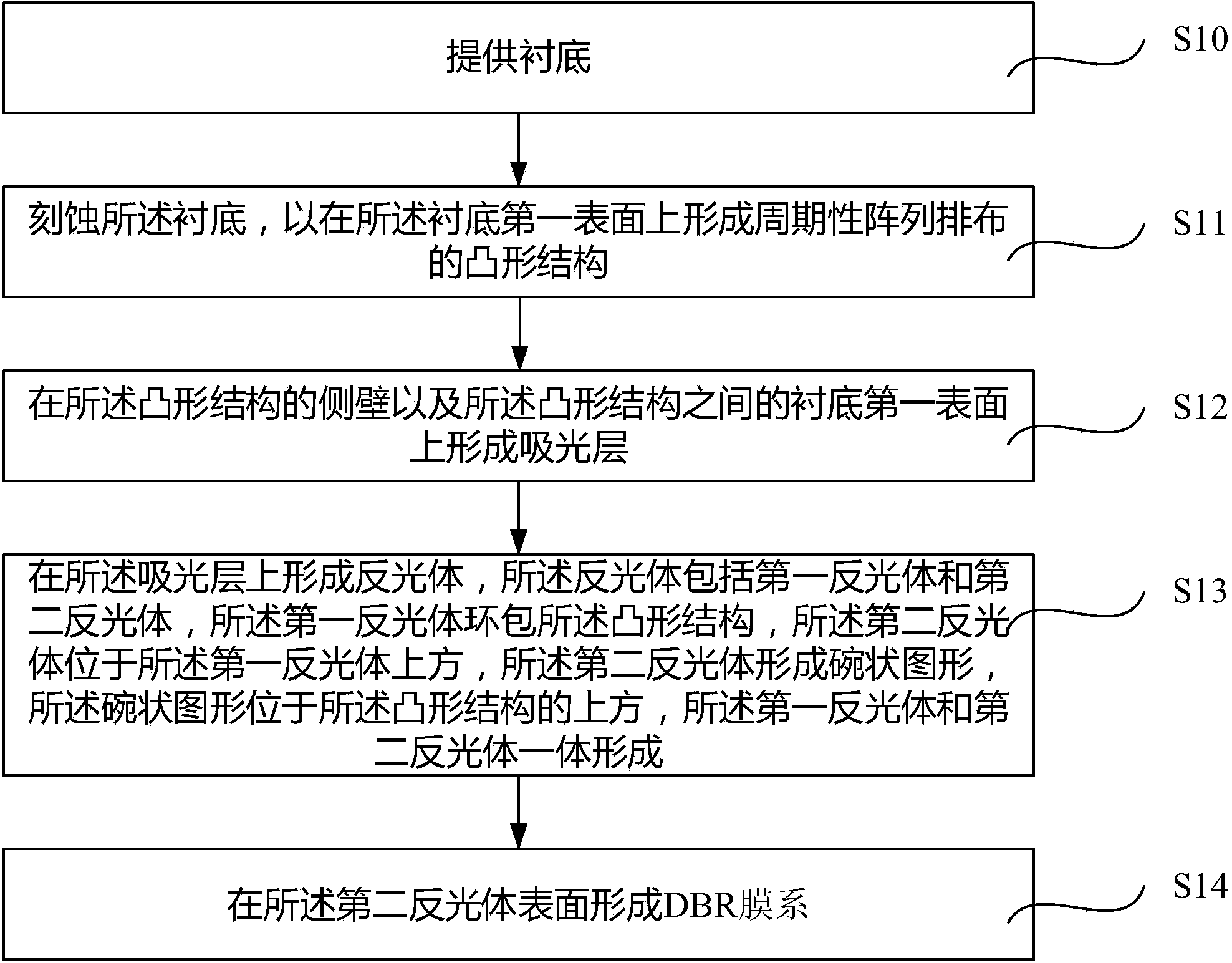
[0056] Please refer to figure 1 , Which is a schematic flow chart of a manufacturing method of an LED substrate structure according to an embodiment of the present invention. Such as figure 1 As shown, the manufacturing method of the LED substrate structure includes:
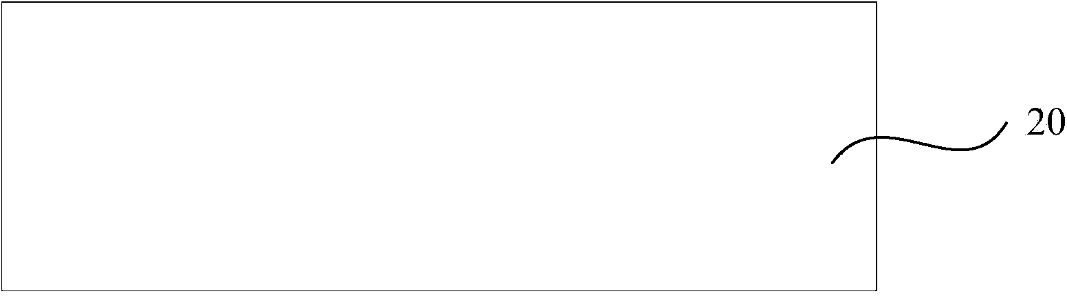
[0057] Step S10: Provide a substrate;

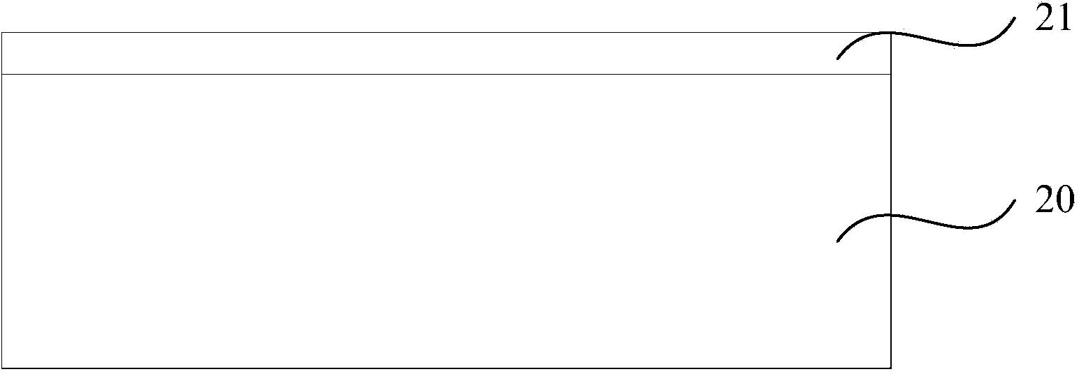
[0058] Step S11: etching the substrate to form convex structures arranged in a periodic array on the first surface of the sub...


PUM

PropertyMeasurementUnit
Thicknessaaaaaaaaaa

Abstract

The invention provides an LED substrate structure and a manufacturing method of the LED substrate structure. The patterned substrate technology and the DRB technology are organically combined, and therefore the luminous efficiency and the luminous brightness of LEDs can be effectively improved. A convex structure is annularly wrapped by a first light reflection body, a DBR film system is arranged on the surface of a second light reflection body, the surface of the convex structure does not have a DBR film system, the axial luminous brightness of the LEDs can be improved while the luminous efficiency and the luminous brightness of the LEDs are improved, and the crystalline quality of the LEDs is not reduced. The convex structure and the DBR film system are located on the same surface of a substrate and are completed before the substrate is thinned, great convenience is brought to machining and follow-up washing, and therefore the implicit cost in the LED machining process is undoubtedly reduced. The manufacturing method of the LED substrate structure is simple in process, low in cost and suitable for large-scale commercial production; the industrialization process for the LEDs to enter the high-end lighting field and homes of common people can be quickened, and the LED substrate structure and the manufacturing method conform to the strategy of the sustainable development of the LEDs.

Description

technical field [0001] The invention relates to the technical field of semiconductor optoelectronic chip manufacturing, in particular to an LED substrate structure and a manufacturing method thereof. Background technique [0002] With the improvement of people's living standards, the enhancement of environmental awareness, and the continuous improvement of the pursuit of home environment, leisure and comfort, lamps and lanterns have gradually shifted from simple lighting functions to the coexistence of lighting and decoration. It is inevitable that solid-state cold light source LED will replace traditional light source and enter people's daily life. [0003] Since the commercialization of GaN-based LEDs in the early 1990s, after more than 20 years of development, its structure has become mature and perfect, and it has been able to meet people's current needs for lighting decoration; but it must completely replace traditional light sources and enter the lighting industry. fi...

Claims


Application Information

Patent Timeline
IPC IPC(8): H01L33/10H01L33/22H01L33/00
CPCH01L33/005H01L33/10H01L33/22
Inventor 丁海生马新刚李东昇李芳芳江忠永
Owner HANGZHOU SILAN AZURE
Why Eureka
Try Eureka