

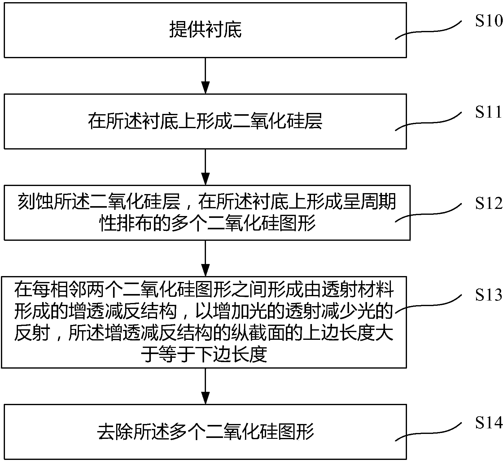
LED substrate structure and manufacturing method of LED substrate structure
A technology of substrate structure and manufacturing method, which is applied in the direction of electrical components, circuits, semiconductor devices, etc., can solve the problems of low light output efficiency of LEDs, and achieve the effects of increasing light output efficiency, increasing axial luminous brightness, and improving luminous brightness
- Summary
- Abstract
- Description
- Claims
- Application Information
AI Technical Summary
Problems solved by technology
Method used
Image

Examples
Embodiment 1
[0051] Specifically, please refer to Figure 2 to Figure 12 , which is a schematic diagram of a device structure formed in the method for manufacturing an LED substrate structure according to Embodiment 1 of the present invention.
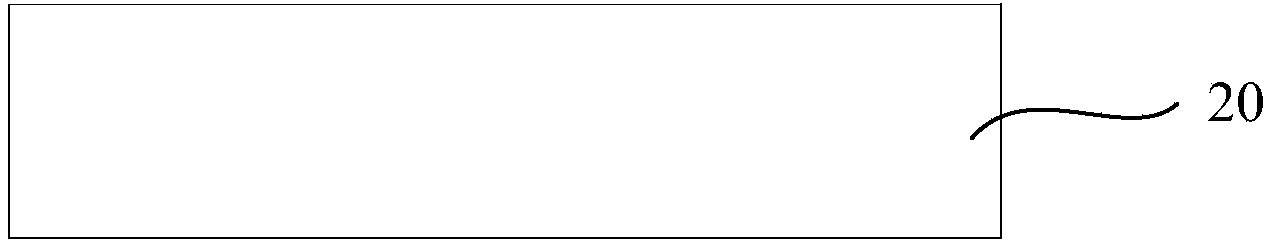
[0052] Such as figure 2 As shown, a substrate 20 is provided, preferably, the substrate 20 is a sapphire substrate.
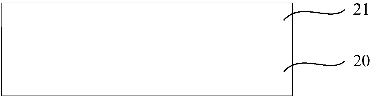
[0053] Next, if image 3 As shown, a silicon dioxide layer 21 is formed on the substrate 20 . In the embodiment of the present application, the thickness of the silicon dioxide layer 21 is 0.5 micrometers to 3 micrometers. Preferably, in forming the silicon dioxide layer 21 on the substrate 20, the deposition speed of the silicon dioxide layer 21 becomes slower and slower, and the process temperature becomes higher and higher. Preferably, the deposition rate of the silicon dioxide layer 21 is gradually decreasing from 100 angstrom / sec to 10 angstrom / sec, and the process temperature is gradually increasing from 200°C to 800°C. ...
Embodiment 2
[0071] Specifically, please refer to Figure 13 to Figure 20 , which is a schematic diagram of the device structure formed in the method for manufacturing the LED substrate structure according to the second embodiment of the present invention.
[0072] Such as Figure 13 As shown, a substrate 30 is provided, preferably, the substrate 30 is a sapphire substrate.
[0073] Next, if Figure 14 As shown, a silicon dioxide layer 31 is formed on the substrate 30 . In the embodiment of the present application, the thickness of the silicon dioxide layer 31 is 0.5 micrometers to 3 micrometers. Preferably, in forming the silicon dioxide layer 31 on the substrate 30, the deposition speed of the silicon dioxide layer 31 becomes slower and slower, and the process temperature becomes higher and higher. Preferably, the deposition rate of the silicon dioxide layer 31 is gradually decreasing from 100 angstrom / sec to 10 angstrom / sec, and the process temperature is gradually increasing from 2...
PUM
 Abstract
Description
Claims
Application Information