A kind of LED structure and manufacturing method thereof

A technology of LED structure and manufacturing method, applied in electrical components, circuits, semiconductor devices, etc., can solve the problems of increased production cost, limited space for brightness improvement, and no improvement in luminous efficiency, and achieves the effect of reducing manufacturing cost and cost.

Active Publication Date: 2017-03-08
HANGZHOU SILAN AZURE
View PDF6 Cites 0 Cited by
  • Summary
  • Abstract
  • Description
  • Claims
  • Application Information

AI Technical Summary

Problems solved by technology

However, patterned substrates replace flat-surfaced sapphire substrates as the mainstream original substrates for LED chips, which undoubtedly increases the production cost of LEDs. Although the increased cost will gradually decrease with the improvement of the patterned substrate production technology level, but but cannot completely eliminate
Moreover, the shape of the final LED is not much improved, and the space for further improving the brightness of the LED is limited.
[0004] With the rapid development of semiconductor integration technology, a LED structure called a high-voltage chip has emerged. Generally, after the epitaxial layer is formed, an isolation groove is formed through a photolithography process, and then placed in the isolation groove. Fill the insulating material, and finally make electrodes on each insulating and separated epitaxial layer to form a series structure; although this structure can improve the luminous brightness of the LED, its luminous efficiency does not actually improve, and it greatly increases the manufacturing cost of the chip manufacturing end.
[0005] Therefore, it is urgent to develop a process technology solution that can replace the formation of isolation grooves first, and then fill the isolation grooves with insulating materials, and can greatly improve LED luminous brightness and production costs, so as to solve the problem that the existing process technology solutions have limited brightness improvement space and production cost. Defect problem with high cost

Method used


Image

  • A kind of LED structure and manufacturing method thereof
  • A kind of LED structure and manufacturing method thereof
  • A kind of LED structure and manufacturing method thereof

Examples


Embodiment 1

[0083] Figure 1 to Figure 8 A schematic diagram of the cross-sectional structure during the fabrication of the patterned substrate provided in this embodiment, Figure 17 It is the flow chart of the patterned substrate manufacturing method of the present embodiment, below in conjunction with Figure 17 and Figure 1-8 A method for forming a patterned substrate according to a specific embodiment of the present invention will be described in detail.

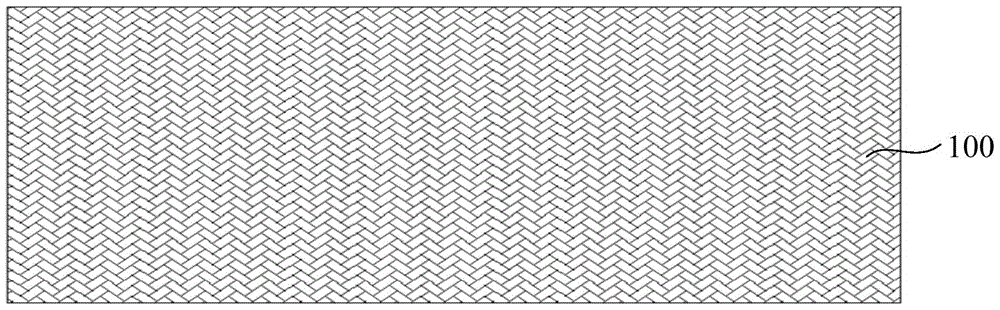
[0084] Such as figure 1 As shown, step S11 is executed to provide an original substrate 100, which may be a silicon carbide (SiC) original substrate, a sapphire (Al2O3) original substrate or a silicon original substrate. In this embodiment, a sapphire substrate is used.

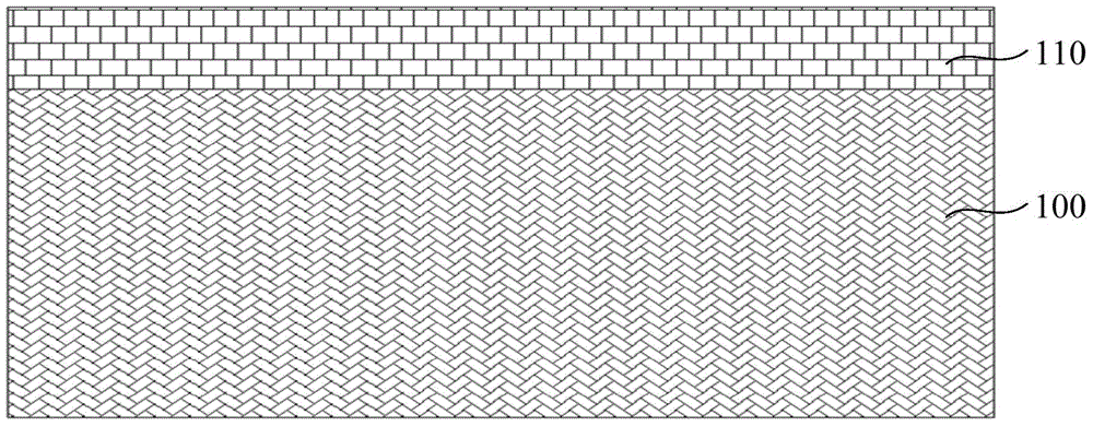
[0085] Such as figure 2As shown, step S12 is performed to form a first mask layer 110 on the original substrate 100 by evaporation, sputtering, spraying, PECVD or LPCVD. Preferably, a first mask layer 110 is formed on the surface of the original substrate ...

Embodiment 2

[0102] Such as Figure 9 As shown, the difference between the patterned substrate provided in this embodiment and the patterned substrate provided in Embodiment 1 lies in that the second pattern structure 102 is a cone-shaped structure.

[0103] In the method for fabricating the patterned substrate of the LED structure provided in this embodiment, on the basis of Embodiment 1, an additional etching for a predetermined time is performed (or the etching time of step S17 is directly extended), and then The second pattern structure 102 is changed from a mesa structure to a cone structure. The specific process parameters can be obtained through limited experiments according to the characteristics of the machine and the requirements of the thickness and corrosion resistance of the silicon dioxide to be formed.

[0104] Wherein, the positional relationship between the original substrate 100 and the first pattern structure 101 , the second pattern structure 102 , and the third patter...

Embodiment 3

[0106] Such as Figure 11 As shown, the difference between the patterned substrate provided by this embodiment and the patterned substrates provided by Embodiments 1 and 2 is that the first pattern structure 101 is a rectangular ring structure and the rectangular ring structure is along the The vertical section (section perpendicular to the surface of the original substrate) of each side in the width direction is triangular, and does not form several second pattern structures 102 and third pattern structures 103 .

[0107] Such as Figure 18 As shown, the method for fabricating the patterned substrate of the LED structure provided in this embodiment includes the following steps:

[0108] Step S31, providing an original substrate 100;

[0109] Step S32, forming a first mask layer 110 on the original substrate 100;

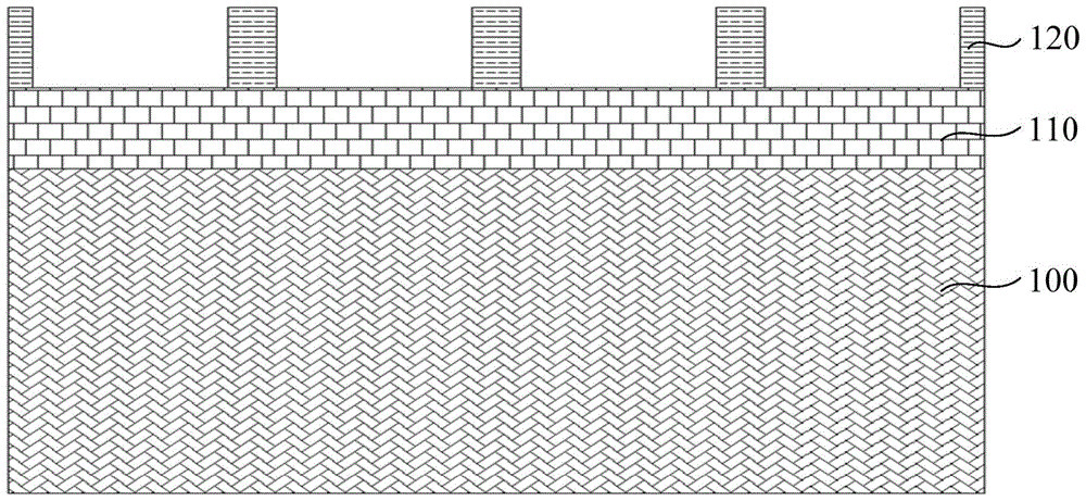
[0110] Step S33, forming a patterned photoresist layer 120 on the first mask layer 110 by a photolithography process, and using the patterned photoresist layer 1...


PUM


Abstract

The invention provides an LED structure and a manufacturing method thereof. A plurality of first graph structures in periodic array configuration are formed in a graphic substrate of the LED structure, the surface of the original substrate is divided into a plurality of areas in periodic array configuration through the first graphic structures, independent light-emitting semiconductor layers are subjected to insulation separation through the graphic substrate during formation, manufacturing of an isolation groove through the lithography etching technology at the chip manufacturing end is omitted, filling of the isolation groove with insulating materials is not needed, first electrodes and second electrodes of independent light-emitting semiconductors are electrically connected as required at same time when the first electrodes and the second electrodes of the independent light-emitting semiconductors are formed, a cascaded structure of an optional number of particles is formed, the independent light-emitting semiconductor layers forming the cascaded structure do not need to be recut, independent packaging of the independent light-emitting semiconductors is subsequentially not needed.

Description

technical field [0001] The invention relates to the field of manufacturing semiconductor photoelectric chips, in particular to an LED structure and a manufacturing method thereof. Background technique [0002] Since its commercialization in the early 1990s, after more than 20 years of development, GaN-based LEDs have been widely used in indoor and outdoor display screens, lighting sources for projection displays, backlight sources, landscape lighting, advertising, traffic instructions, etc. Field, and known as the most competitive new generation of solid-state light source in the 21st century. However, for the semiconductor light-emitting device LED, to replace the traditional light source and enter the high-end lighting field, two factors must be considered: one is to increase the luminous brightness, and the other is to reduce the production cost. [0003] In recent years, various technologies have emerged to improve the brightness of LEDs, such as patterned substrate tec...

Claims


Application Information

Patent Timeline
Patent Type & Authority Patents(China)
IPC IPC(8): H01L33/22H01L33/36H01L33/00
CPCH01L33/005H01L33/22H01L33/385H01L2933/0008H01L2933/0016
Inventor 丁海生马新刚李东昇李芳芳江忠永
Owner HANGZHOU SILAN AZURE
Why Eureka
Try Eureka