Plasma processing apparatus including an isothermal processing zone

A technology of plasma and processing area, which is applied in semiconductor/solid-state device manufacturing, coating, gaseous chemical plating, etc., and can solve problems such as uneven substrate processing

Active Publication Date: 2015-01-14
LAM RES CORP
View PDF9 Cites 9 Cited by
  • Summary
  • Abstract
  • Description
  • Claims
  • Application Information

AI Technical Summary

Problems solved by technology

In such chambers, uneven heating across the semicondu

Method used


Image

  • Plasma processing apparatus including an isothermal processing zone
  • Plasma processing apparatus including an isothermal processing zone
  • Plasma processing apparatus including an isothermal processing zone

Examples


Embodiment approach

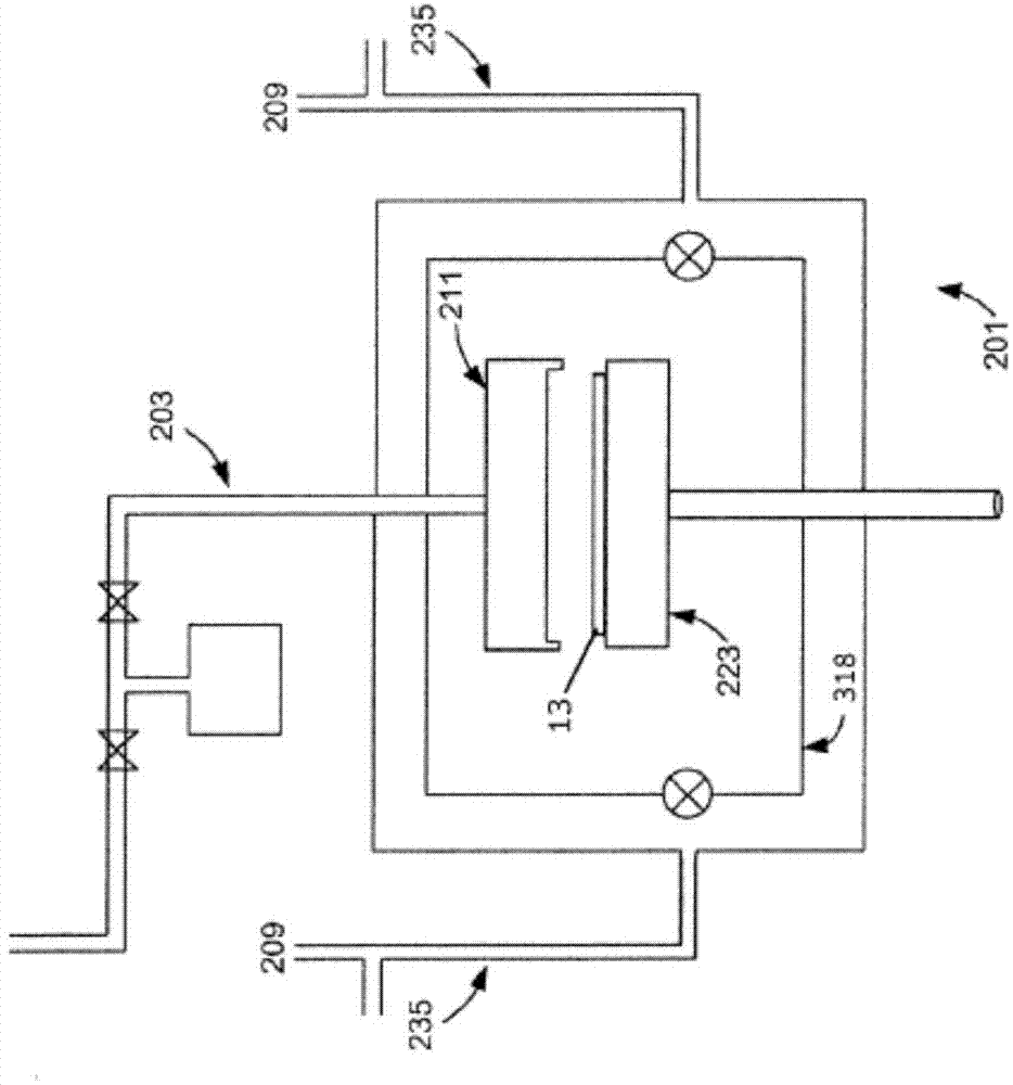
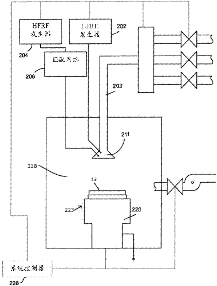
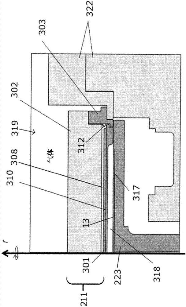
[0025] image 3 A cross-section of the chemical isolation chamber 319 is shown in more detail, including figure 1 and figure 2 The pedestal module 223 and the showerhead module 211, wherein the pedestal module 223 and the showerhead module 211 form a cavity 318 in which the semiconductor substrate is processed. The cavity 318 is formed between the showerhead module 211 and the base module 223, wherein the lower surface of the panel 301 of the showerhead module 211 forms the upper wall and the sidewall of the cavity 318, and the upper surface of the base module 223 forms the upper wall of the cavity 318. lower wall. An exemplary embodiment of a deposition apparatus including a dual chamber seal can be found in commonly assigned US Patent 7,737,035, which is incorporated herein by reference in its entirety.

[0026] The base module 223 includes a bottom RF electrode 317 on which the substrate 13 rests. Preferably, the bottom RF electrode 317 is grounded. During processing,...


PUM


Abstract

A deposition apparatus for processing semiconductor substrates having an isothermal processing zone comprises a chemical isolation chamber in which semiconductor substrates are processed. A process gas source is in fluid communication with a showerhead module which delivers process gases from the process gas source to the isothermal processing zone wherein the showerhead module includes a faceplate wherein a lower surface of the faceplate forms an upper wall of a cavity defining the isothermal processing zone, a backing plate, and an isolation ring which surrounds the faceplate and the backing plate. At least one compression seal is compressed between the faceplate and the backing plate which forms a central gas plenum between the faceplate and the backing plate. A substrate pedestal module is configured to heat and support a semiconductor substrate wherein an upper surface of the pedestal module forms a lower wall of the cavity defining the isothermal processing zone within the chemical isolation chamber. A vacuum source is in fluid communication with the isothermal processing zone for evacuating process gas from the processing zone.

Description

technical field [0001] The present invention pertains to apparatus for performing chemical deposition and may find particular use in the process of performing plasma-enhanced chemical deposition of thin films. Background technique [0002] Plasma processing equipment is used to treat semiconductor substrates by the following techniques: Etching, Physical Vapor Deposition (PVD), Chemical Vapor Deposition (CVD), Plasma Enhanced Chemical Vapor Deposition (PECVD), Atomic Layer Deposition (ALD), Plasma Enhanced Atomic layer deposition (PEALD), pulsed layer deposition (PDL), plasma enhanced pulsed layer deposition (PEPDL) processing and resist stripping. A type of plasma processing apparatus used in plasma processing includes a reaction chamber including a top electrode and a bottom electrode. Radio frequency (RF) power is applied between the electrodes to energize a process gas into a plasma for processing the semiconductor substrate in the reaction chamber. In such chambers, u...

Claims


Application Information

Patent Timeline
IPC IPC(8): H01L21/00H01L21/3065H01J37/32
CPCH01L21/02274H01L21/0262H01L21/0228C23C16/45565H01L21/67011H01L21/02271C23C16/509
Inventor 拉梅什·钱德拉赛卡兰杰里米·塔克卡尔·利泽艾伦·斯考普
Owner LAM RES CORP
Why Eureka
Try Eureka