
Liquid crystal panel and method for manufacturing liquid crystal panel

A liquid crystal panel, inner surface technology, applied in nonlinear optics, instruments, optics, etc., can solve the problems of rapid decline in display effect and TFT deterioration of display panels, and achieve the effect of preventing rapid deterioration, excellent product characteristics, and reasonable structure

Inactive Publication Date: 2017-10-03
BOE TECH GRP CO LTD +1
View PDF6 Cites 0 Cited by
  • Summary
  • Abstract
  • Description
  • Claims
  • Application Information

AI Technical Summary

Problems solved by technology

For example, the display effect of a certain display panel decreases rapidly, and the test shows that the reason is that the TFT deteriorates rapidly during use.

Method used


Image

  • Liquid crystal panel and method for manufacturing liquid crystal panel
  • Liquid crystal panel and method for manufacturing liquid crystal panel
  • Liquid crystal panel and method for manufacturing liquid crystal panel

Examples


Embodiment 1

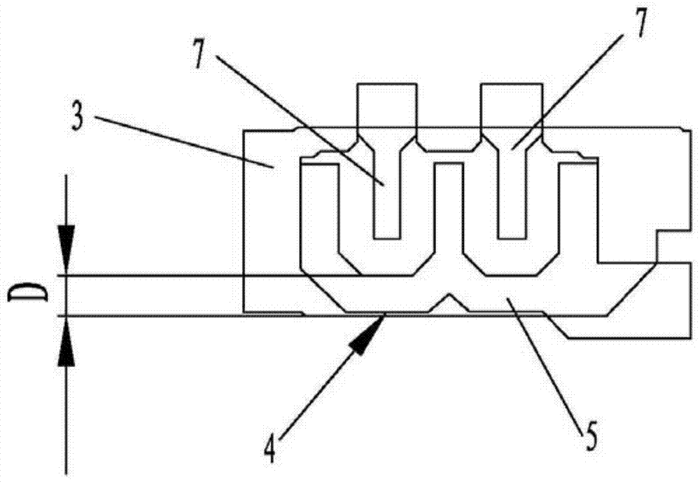
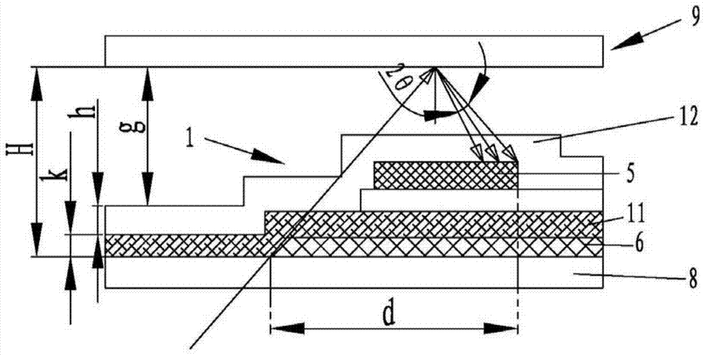
[0050] Such as figure 1 , figure 2As shown, the embodiment of the liquid crystal panel of the present invention includes an array substrate 1 and a box-matched substrate 9 that is boxed with the array substrate 1, and a plurality of data lines (not shown in the figure) and a plurality of gate lines are arranged on the array substrate 1 3. A plurality of data lines intersect with a plurality of gate lines 3 to define a plurality of pixel areas; the array substrate 1 also includes a plurality of TFTs, and the TFTs include a source 5, a drain 7, and a gate 6, and the area occupied by at least one TFT Including the opaque area containing the channel area 4, the distance D between the boundary of the channel area 4 and the boundary of the opaque area in the direction parallel to the liquid crystal panel is greater than or equal to the set distance d.

[0051] In an embodiment of the liquid crystal panel of the present invention, the opaque region may be formed by an opaque gate l...

Embodiment 2

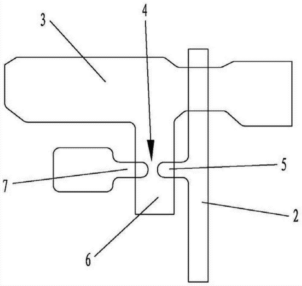
[0079] Such as image 3 , Figure 4 As shown, in the embodiment of the liquid crystal panel of the present invention, a plurality of data lines 2 are arranged on the array substrate 1, the TFT includes a gate 6 connected to the gate line 3, and the projection of the channel region of the TFT is located where the gate 6 is located. In the region, the boundary of the opaque region includes the boundary of the source 5 on the side away from the channel region 4 and the boundary of the drain 7 on the side away from the channel region 4 .

[0080] The width of the area formed by the source electrode 5, the drain electrode 7 and the channel region 4 is greater than the width of the gate 6, and the channel region 4 is an elongated region (for example, refers to the gap formed between the source electrode and the drain electrode. image 3 exemplarily shown as an elongated area in the up-down direction).

[0081] In an embodiment of the manufacturing method of the liquid crystal pane...


PUM


Abstract

The invention relates to a liquid crystal display panel and a manufacturing method of the liquid crystal display panel. The liquid crystal display panel comprises an array substrate and a box-to-box substrate; a plurality of TFTs (Thin Film Transistors) are arranged on the array substrate; a region occupied by at least one TFT comprises a non-transparent region containing a channel region; the distance between the boundary of the channel region and the boundary of the non-transparent region in the direction parallel to the liquid crystal display panel is greater than or equal to a set distance d. The manufacturing method of the liquid crystal display panel disclosed by the invention comprises the step of calculating the minimum distance d' between the boundary of the channel region and the boundary of the non-transparent region in the direction parallel to the liquid crystal display panel. Through the technical scheme, the TFTs are effectively prevented from being quickly degraded in use, and thus the design and production efficiency of the liquid crystal display panel is promoted. Related products manufactured by utilizing the manufacturing method of the liquid crystal display panel disclosed by the invention are more reasonable in structure and more excellent in product feature.

Description

technical field [0001] The invention relates to the field of liquid crystal display, in particular to a liquid crystal panel and a method for manufacturing the liquid crystal panel. Background technique [0002] In flat panel display (FPD, Flat Panel Display) technology, liquid crystal display (LCD, LiquidCrystal Display) has gradually replaced cathode ray tube display and has become the mainstream display due to its advantages of thinness, lightness, compactness, and space saving. Among various types of LCDs, TFT-LCD (Thin Film Transistor-Liquid Crystal Display) is a kind of active matrix type liquid crystal display. TFT-LCD has excellent performance and is suitable for large-scale automatic production , and the cost of raw materials is low, so it occupies an important position in LCD. [0003] In the manufacturing process of TFT-LCD, the product design is related to the performance of the product after the final production. Among them, the design of the TFT of the LCD pan...

Claims


Application Information

Patent Timeline
Patent Type & Authority Patents(China)
IPC IPC(8): G02F1/1362G02F1/1368G02F1/1333
CPCG02F1/1333G02F1/136286G02F1/1368G02F1/136295
Inventor 封宾洪永泰
Owner BOE TECH GRP CO LTD
Learn More