LED chip and application thereof

A LED chip and chip technology, which is applied in the direction of electrical components, circuits, semiconductor devices, etc., can solve the problems of low photoelectric conversion efficiency and environmental temperature sensitivity, and achieve the effect of insensitivity to environmental temperature and improving photoelectric conversion efficiency

Inactive Publication Date: 2015-02-18
SUZHOU INST OF NANO TECH & NANO BIONICS CHINESE ACEDEMY OF SCI
View PDF6 Cites 0 Cited by
  • Summary
  • Abstract
  • Description
  • Claims
  • Application Information

AI Technical Summary

Problems solved by technology

[0004] The main purpose of the present invention is to provide a LED chip with a new packaging mode and its use method, so as to solve the technical problems in the prior art that the LED chip is sensitive to ambient temperature and the photoelectric conversion efficiency becomes low over time.

Method used


Image

  • LED chip and application thereof
  • LED chip and application thereof
  • LED chip and application thereof

Examples


Embodiment Construction

[0020] The technical solutions in the embodiments of the present invention will be described in detail below in conjunction with the accompanying drawings in the embodiments of the present invention. Obviously, the described embodiments are only some of the embodiments of the present invention, not all of them. Based on the embodiments of the present invention, all other embodiments obtained by persons of ordinary skill in the art without making creative efforts belong to the protection scope of the present invention.

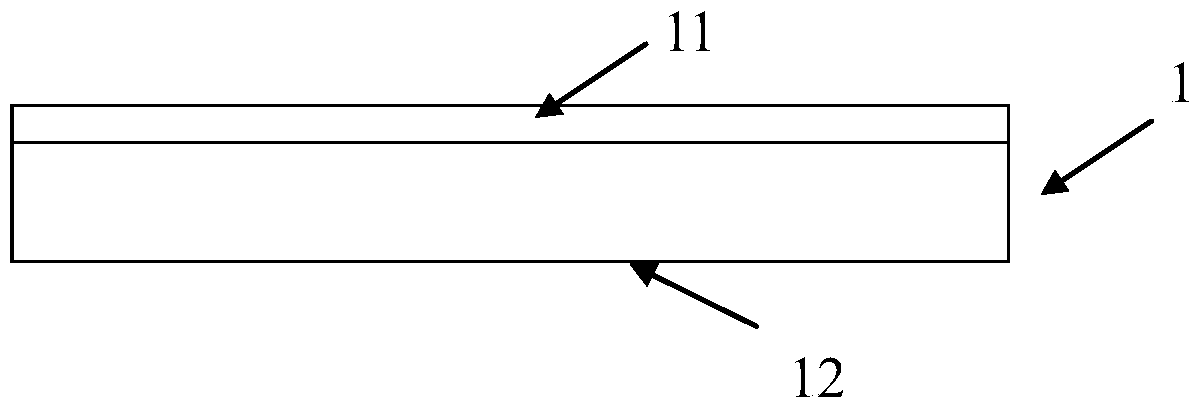
[0021] see figure 1 One aspect of the present invention provides an LED chip 1, comprising a substrate 11 and an epitaxial layer 12 distributed on the surface of the substrate, the size of any one of the long side and wide side of the LED chip is greater than 7mil (density ear), that is, 177.8 μm.

[0022] Further, the LED chip can be an LED chip of various materials and structures known in the industry, for example, a LED chip with a front-mounted, flip-chip,...


PUM

PropertyMeasurementUnit
Sizeaaaaaaaaaa

Abstract

The invention discloses an LED chip and application thereof. The LED chip comprises a substrate and an epitaxy layer distributed on the surface of the substrate, either the length or the width of the LED chip is larger than 177.8 micrometers. When the LED chip is rectangular, the ratio of the length to the width is larger than or equal to 1.5:1. The using method of the LEDS chip includes applying operating current to the LED chip so as to let the LED chip emit light, wherein the current density applied on the LED chip is smaller than 120mA / mm2. By the aid of the LED chip, photoelectric conversion efficiency of the LED chip can be effectively improved, and the LED chip is insensitive to the environmental temperature and has no problem that LED transient light effect is weakened over time. Meanwhile, the LED chip can be packaged in any packaging structure and is particularly applicable to the transparent packaging structure.

Description

technical field [0001] The invention particularly relates to a novel LED chip with high photoelectric conversion efficiency and insensitive to surrounding temperature and its application. Background technique [0002] The first LED product was born in the United States in the 1960s. Its appearance has brought a lot of brilliance to people's lives. Due to the advantages of LEDs such as long life, low power consumption, and environmental protection, related technologies have developed very rapidly. . It has become a "ubiquitous" optoelectronic device and light source that is closely related to our lives, such as the backlight of mobile phones, traffic lights, large-screen full-color display screens and lights for landscape lighting, etc. [0003] However, there are still many factors restricting the further application and development of LEDs. For example, the existing LED chips are usually more sensitive to the temperature of the working environment. In other words, the amb...

Claims


Application Information

Patent Timeline
IPC IPC(8): H01L33/48H01L31/0352
CPCH01L33/48H01L33/005H01L2933/0033
Inventor 梁秉文陈怡敏张涛
Owner SUZHOU INST OF NANO TECH & NANO BIONICS CHINESE ACEDEMY OF SCI
Why Eureka
Try Eureka