Method of fabricating photovoltaic devices with reduced conduction band shift between pnictide absorber and emitter films

一种导带偏移、元素化的技术,应用在改善这些异质结的质量领域,能够解决材料不同、不能达到性能水平等问题,达到高开路电压、改进电子性能、高效率的效果

Inactive Publication Date: 2016-12-21
DOW GLOBAL TECH LLC +1
View PDF3 Cites 0 Cited by
  • Summary
  • Abstract
  • Description
  • Claims
  • Application Information

AI Technical Summary

Problems solved by technology

[0008] Therefore, despite the use of n-type materials such as ZnS and p-type materials such as Zn in photovoltaic junctions 3 P 2 Potential advantages of combinations, but the materials are too different to achieve higher performance levels

Method used


Image

  • Method of fabricating photovoltaic devices with reduced conduction band shift between pnictide absorber and emitter films

Examples


Embodiment 1

[0082] Embodiment 1: substrate preparation

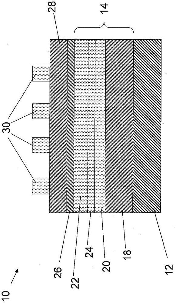
[0083] According to the techniques described in more detail in co-pending U.S. Provisional Patent Application Serial No. 61 / 441,997, filed February 11, 2011, in the name of Kimball et al., and corresponding apparatus for implementing these techniques, in degenerate doping ( Degeneratively doped) on p-type GaAs(001) single crystal substrate using compound source, molecular beam epitaxy (MBE) technology to fabricate solid ZnS / Zn 3 P 2 HETEROJUNCTION SOLAR CELLS, said application titled METHODOLOGY FOR FORMINGPNICTIDE COMPOSITIONS SUITABLE FOR USE IN MICROELECTRONIC DEVICES, Attorney Docket No. 70360 (DOW 0039P1). The growth was performed in an ultra-high vacuum (UHV) molecular beam epitaxy chamber at 10 -10 The base pressure of the support is carried out. The chamber is equipped with Zn 3 P 2 and ZnS compound sources, and Al, Ag, Zn and Mg element sources.

[0084] The back side of the GaAs substrate is coated with a Pt-Ti-Pt lo...

Embodiment 2

[0086] Example 2: Zinc Phosphide Growth

[0087] ZnP film growth by sublimation of 99.9999% Zn from a Knudsen effusion cell 3 P 2 conduct. The effusion chamber is heated to over 350°C, providing a 5x10 -7 and 2x10 -6 The beam pressure between Torr was measured by a translatable bare ionization manometer. The growth was performed at a substrate temperature of 200°C. The film deposition rate is about 0.3 to 1.0 Angstroms / s. Typical film thicknesses are 400 to 500 nm. Thicker films are possible, but require longer growth rates or higher beam pressures. Elemental Ag is incorporated as a dopant during the growth process by co-sublimation from an additional Ag source. The Ag source was operated between 700°C and 900°C. in Zn 3 P 2 Immediately after growth, the substrate temperature was lowered to the ZnS deposition temperature.

Embodiment 3

[0088] Example 3: Regulated ZnS Growth

[0089] ZnS growth was performed using a Knudsen effusion chamber containing 99.9999% ZnS. The effusion chamber was heated to 850°C for deposition. This yields about 1.5x10 -6 Torr beam pressure. During ZnS growth, the substrate was kept at 100°C. At this beam pressure and substrate temperature, the ZnS growth rate is about 1 Angstrom / s. A film with a thickness of 100 nm was grown. Al and Mg were co-introduced together with ZnS during growth. Al was provided using an electron beam evaporator filled with 99.9999% Al metal. The degree of Al incorporation and thus dopant density is controlled by the power supplied to the evaporator. The Al density in the grown film is typically 1x10 18 and 1x10 19 cm -3 between. Mg was supplied at an operating temperature between 300°C and 600°C using an effusion chamber filled with 99.9999% Mg. Mg was only co-introduced during the first 10 to 100 nm of film growth. In an alternative embodiment...


PUM

PropertyMeasurementUnit
band gapaaaaaaaaaa
band gapaaaaaaaaaa

Abstract

The principles of the present invention are used to reduce the conduction band shift between chalcogenide emitter and phosphonide absorber films. Alternatively, the present invention provides a strategy to more closely match the electron affinity properties between the absorber and emitter components. The resulting photovoltaic device has the potential to have higher efficiency and higher open circuit voltage. The resistance of the resulting junction will decrease as current leakage decreases. In an illustrative implementation, the present invention incorporates one or more modulators into the emitter layer to modulate electron affinity properties, thereby reducing the conduction band shift between the emitter and the absorber. In the case of n-type emitters such as ZnS or ternary compounds such as zinc selenide sulfide (optionally doped with Al), etc., when the absorber is a p-type phosphoride material such as zinc phosphide or doped with other than Zn When phosphating a zinc alloy with at least one other metal and optionally at least one non-metal other than phosphorus, an exemplary modifier is Mg. Therefore, photovoltaic devices including such films exhibit improved electronic performance.

Description

[0001] priority [0002] This application claims priority under 35 U.S.C. §119(e) to U.S. Provisional Application No. 61 / 592,957, filed January 31, 2012, entitled "METHOD OF MAKING PHOTOVOLTAIC DEVICES WITHREDUCED CONDUCTION BAND OFFSET BETWEEN PNICTIDE ABSORBER FILMS AND EMITTER FILMS (Method of Fabricating Photovoltaic Devices with Reduced Conduction Band Offset Between Pnictide Absorber and Emitter Films)", the entirety of which application is hereby incorporated by reference for all purposes. technical field [0003] The present invention relates to a method of forming a solid state junction comprising a p-type pnictide semiconductor absorber composition and an n-type Group II / VI composition. More specifically, the present invention relates to methods of improving the quality of these heterojunctions by incorporating in the emitter agents that reduce the conduction band shift between the absorber and the emitter. Background technique [0004] Pnictide-based semiconduct...

Claims


Application Information

Patent Timeline
Patent Type & Authority Patents(China)
IPC IPC(8): H01L31/0224H01L31/032H01L31/072H01L31/18
CPCH01L31/022466H01L31/032H01L31/072H01L31/18Y02E10/50
Inventor J·P·伯斯科G·M·金伯尔H·A·阿特瓦特N·S·刘易斯R·克里斯廷-利格曼菲斯特M·W·德格鲁特
Owner DOW GLOBAL TECH LLC
Why Eureka
Try Eureka