Monolithic integrated laser chip based on amplification feedback to realize straight-strip bandwidth expansion

A monolithic integration and bandwidth expansion technology, which is applied in the device for controlling the output parameters of the laser, the structure of the optical resonator, etc., which can solve the problem of the limited adjustment range of the feedback intensity, the difficulty of finding the direct modulation bandwidth expansion, and the increase of workload and cost. and other problems to achieve the effect of direct adjustment response bandwidth expansion

Active Publication Date: 2015-02-25
INST OF SEMICONDUCTORS - CHINESE ACAD OF SCI
View PDF6 Cites 19 Cited by
  • Summary
  • Abstract
  • Description
  • Claims
  • Application Information

AI Technical Summary

Problems solved by technology

However, the feedback area of ​​this structure only contains a phase adjustment area, and there is no additional feedback intensity adjustment area, which makes the adjustment range of the feedback intensity very limited
This will greatly limit the practical use of lasers. After all, a suitable feedback strength directly determines whether the device can achieve bandwidth expansion.
At the same time, for this structure, if we need to find a specific optical-optical response oscillation peak (bandwidth extension peak), we need to accurately select the laser chip cavity length, which will increase the workload and cost
And in practice, we have also tested a large number of chips with DFB laser region plus passive phase region structure, and the result is that it is difficult to find the phenomenon of direct modulation bandwidth expansion

Method used


Image

  • Monolithic integrated laser chip based on amplification feedback to realize straight-strip bandwidth expansion
  • Monolithic integrated laser chip based on amplification feedback to realize straight-strip bandwidth expansion
  • Monolithic integrated laser chip based on amplification feedback to realize straight-strip bandwidth expansion

Examples


Embodiment Construction

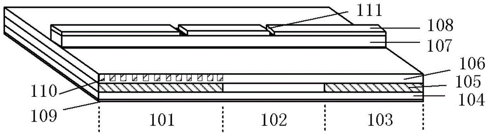
[0020] see figure 1 As shown, the present invention provides a monolithic integrated laser chip that realizes direct modulation bandwidth expansion based on amplification feedback, including:

[0021] A lower confinement layer 104, the material of the lower confinement layer 104 is InGaAsP, which is used to confine carriers and photons in the vertical direction, with a thickness of 80 to 150 nm;

[0022] An active layer 105, which is fabricated on the lower confinement layer 104 and used to convert electrical energy into photons, is made of lightly doped InGaAsP or AlGaInAs quaternary material with a thickness of 80nm to 100nm. The active region layer 105 is preferably a multi-quantum well active region layer, the material is preferably an AlGaInAs quaternary material, and the gain peak corresponds to the 1310nm or 1550nm band;

[0023] An upper confinement layer 106, which is formed on the active layer 105, the material of the upper confinement layer 106 is InGaAsP, and the ...


PUM


Abstract

A monolithic integrated laser chip based on amplification feedback to realize straight-strip bandwidth expansion comprises a lower limiting layer, an active layer, an upper limiting layer, a waveguide layer, a P+electrode layer and an N+electrode layer. The active layer is manufactured on the lower limiting layer, the upper limiting layer is manufactured on the active layer, the waveguide layer is strip-shaped and longitudinally manufactured in the middle of the front of the upper limiting layer, the P+electrode layer is divided into three sections by isolating grooves and manufactured on the waveguide layer, the N+electrode layer is manufactured on the back of the lower limiting layer, the three sections of the P+electrode layer are a DFB (distributed feedback Bragg) laser area, a passive phase adjusting area and an active amplification feedback area respectively, a distribution feedback Bragg grating layer is manufactured on a portion, corresponding to the upper limiting layer, of the DFB laser area, and gain peak between the active layer corresponding to the passive phase adjusting area and the active layer corresponding to the DFB laser area and the active amplification feedback area has 90nm of blue shift. The monolithic integrated laser chip can break through limitation of straight-strip bandwidth of a common laser chip, and laser straight-strip bandwidth expansion can be realized through a method which is ingenious, effective and low in cost.

Description

technical field [0001] The invention relates to the field of semiconductor optoelectronics, in particular to a monolithic integrated laser chip that realizes direct modulation bandwidth expansion based on amplification feedback. Background technique [0002] In the current optical communication system, large-capacity data is transmitted using light, while the storage and processing of signals are still electrical media. The process of loading high-speed electrical signals onto light waves through high-speed modulators or light sources is modulation. modulation. The two main modulation methods are direct modulation and external modulation. The former modulates the light intensity by changing the magnitude of the laser injection current, and the latter uses an external optical modulator to modulate the continuous light emitted by the semiconductor laser. Externally modulated transmitters are the main solution for medium and long-distance Dense wavelength division multiplexing...

Claims


Application Information

Patent Timeline
Patent Type & Authority Applications(China)
IPC IPC(8): H01S5/12H01S5/06
Inventor 余力强吉晨赵玲娟陆丹王浩郭露
Owner INST OF SEMICONDUCTORS - CHINESE ACAD OF SCI
Why Eureka
Try Eureka