Organic light-emitting diode display device

A technology of light-emitting diodes and display devices, which is applied in the direction of diodes, optics, nonlinear optics, etc., can solve the problems of viewing and displaying image interference, failing to meet the viewing needs of viewers, and affecting the viewing effect of viewers, so as to meet the needs of viewing and use Effect

Active Publication Date: 2015-03-04
KUSN INFOVISION OPTOELECTRONICS
View PDF5 Cites 16 Cited by
  • Summary
  • Abstract
  • Description
  • Claims
  • Application Information

AI Technical Summary

Problems solved by technology

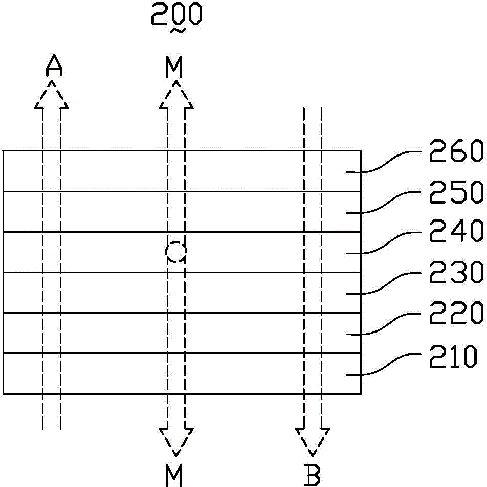
[0003] However, when the OLED display panel 200 is in a situation where the external ambient light is strong, the strong external ambient light A or B enters the OLED display panel 200 from the transparent substrate 210 or the transparent cathode 260 and exits from the transparent cathode 260 or the transparent substrate 210, It will cause great interference to the viewer watching the displayed image, thus affecting the viewing effect of the viewer
Using the OLED display panel 200, it is impossible to choose not to view the environment image on the side of the transparent substrate 210 or the transparent cathode 260 of the OLED display panel 200 according to the needs, which cannot meet the viewing needs of the viewer.

Method used


Image

  • Organic light-emitting diode display device
  • Organic light-emitting diode display device
  • Organic light-emitting diode display device

Examples


Embodiment Construction

[0025] In order to further illustrate the technical means adopted by the present invention to achieve the intended invention purpose

[0026] Section and effect, below in conjunction with accompanying drawing and preferred embodiment, to the organic that proposes according to the present invention

[0027] The specific implementation, structure, characteristics and efficacy of light-emitting diode display devices, in detail

[0028] described as follows:

[0029] The aforementioned and other technical contents, features and effects of the present invention will be clearly presented in the following detailed description of preferred embodiments with reference to the drawings. Through the description of specific implementation methods, the technical means and effects of the present invention to achieve the intended purpose can be understood more deeply and specifically, but the attached drawings are only for reference and description, and are not used to explain the present inv...


PUM


Abstract

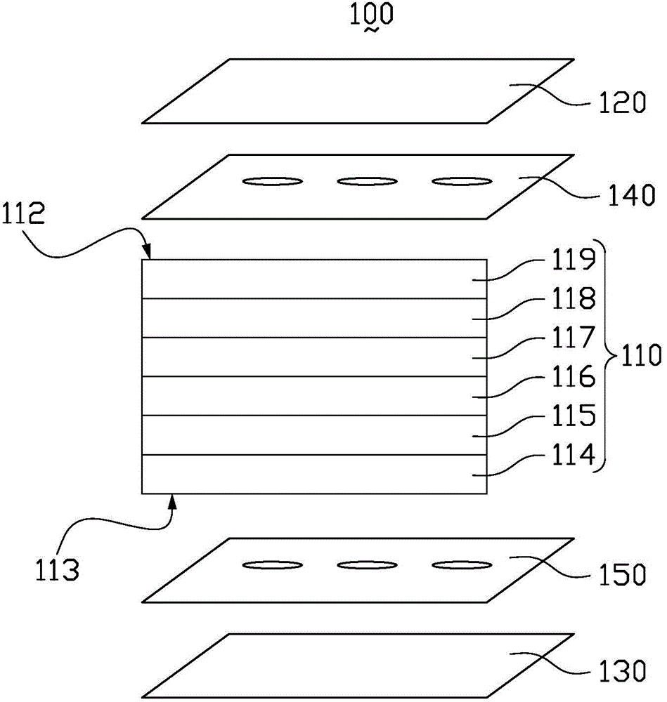
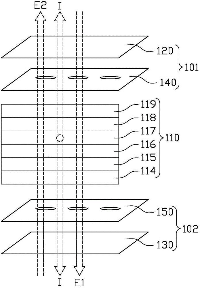
The invention discloses an organic light-emitting diode display device which comprises an organic light-emitting diode display panel, a first polarizer, a second polarizer, a first liquid crystal layer and a second liquid crystal layer. The organic light-emitting diode display panel is provided with a first side and a second side which are opposite to each other, the first polarize is arranged on the first side of the organic light-emitting diode display panel and has a first polarization direction, and the second polarizer is arranged on the second side of the organic light-emitting diode display panel and has a second polarization direction which is orthogonal to the first polarization direction. The first liquid crystal layer is arranged between the first polarizer and the organic light-emitting diode display panel and can be in working states which include a first state and a second state, the second liquid crystal layer is arranged between the second polarizer and the organic light-emitting diode display panel and can be in working states which include a first state and a second state, and the working states of the second liquid crystal layer are identical to the working states of the first liquid crystal layer. The organic light-emitting diode display device has the advantages that the display working stages can be freely switched over as needed, and accordingly double-side transparent display or double-side display effects can be realized.

Description

technical field [0001] The invention relates to the field of display technology, in particular to an organic light emitting diode display device. Background technique [0002] figure 1 It is a structural schematic diagram of an existing organic light-emitting diode (Organic Light-Emitting Diode, OLED) display device. Such as figure 1 As shown, the OLED display panel 200 includes a transparent substrate 210 and a transparent anode 220 , a hole transport layer 230 , a light emitting layer 240 , an electron transport layer 250 and a transparent cathode 260 sequentially disposed on the transparent substrate 210 . Wherein, when a certain driving voltage is applied to the transparent anode 220 and the transparent cathode 260, electrons and holes are respectively injected from the transparent cathode 260 and the transparent anode 220 into the electron transport layer 250 and the hole transport layer 230, and the electrons and holes pass through the electron transport layer 250 an...

Claims


Application Information

Patent Timeline
Patent Type & Authority Applications(China)
IPC IPC(8): G02F1/1347G02F1/1335H01L27/32
CPCG02F1/1335G02F1/1347H10K59/50
Inventor 崔宏青
Owner KUSN INFOVISION OPTOELECTRONICS
Why Eureka
Try Eureka